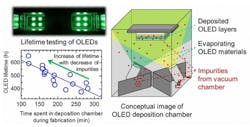
For OLEDs, minuscule amounts of impurities in deposition vacuum can greatly reduce device lifetime
Reproducibility is a necessity for science and manufacturing but has long eluded researchers studying the lifetime of organic light-emitting diodes (OLEDs). New research sheds light on the cause: impurities that are present in the vacuum chamber during the fabrication of OLEDs but in amounts so small that they are easily overlooked.
Researchers from the Center for Organic Photonics and Electronics Research (OPERA), Japan Science and Technology Agency (JST), and Kyushu University (all in Fukuoka, Japan); Sumika Chemical Analysis Service (Niihama and Osaka, Japan); and the Institute of System Information Technology and Nanotechnology (ISIT; Sawara, Japan) discovered that OLED lifetime sharply increases when the time an OLED must spend in the vacuum chamber during fabrication is reduced.1
Plasticizers are a problem
Using liquid chromatography-mass spectrometry to identify the impurities, the researchers found that many could be traced to previously deposited materials and plasticizers from the vacuum-chamber components themselves. While control of water content has been known to be important for improving lifetime, these new results show that impurities amounting to less than even a single molecular layer from sources such as the fabrication chamber itself must be closely managed to reproducibly achieve highly stable and reliable devices.
The researchers note that longer OLED lifetimes could be achieved both by better cleaning of the vacuum chambers before use and by vacuum-chamber designs that minimize the use of resin materials that can release plasticizers into the vacuum chamber.
Source: https://www.kyushu-u.ac.jp/en/researches/view/40
REFERENCE:
1. Hiroshi Fujimoto et al., Scientific Reports (2016); doi:10.1038/srep38482

John Wallace | Senior Technical Editor (1998-2022)
John Wallace was with Laser Focus World for nearly 25 years, retiring in late June 2022. He obtained a bachelor's degree in mechanical engineering and physics at Rutgers University and a master's in optical engineering at the University of Rochester. Before becoming an editor, John worked as an engineer at RCA, Exxon, Eastman Kodak, and GCA Corporation.
