At OFC 2017 (March 19 to 23; Los Angeles, CA), Imec (Leuven, Belgium) has unveiled a 896 Gbit/s silicon photonics transceiver of just a few square millimeters in area, targeting future Tbit/s optical links. The achievement highlights the scalability of Imec's iSiPP50G silicon photonics platform, paving the way for next-generation short-reach optical interconnects.
Driven by exponential demand for interconnect bandwidth in datacenters, single-mode optical transceivers will need to scale to Tbit/s capacity and be tightly integrated with network switches. Silicon photonics (SiPh) has been identified as a promising technology platform to realize such aggressive bandwidth and integration targets, substantially going beyond 100 Gbit/s technology available today.
In the work presented at OFC, Imec combines recently developed 50 GHz active optical components with a multicore fiber interface to show a proof-of-concept 896 Gbit/s spatial-division multiplexing SiPh transceiver.
GeSi technology
The bidirectional transceiver combines dense arrays of 56 Gbit/s germanium-silicon (GeSi) electroabsorption modulators (EAMs) and GeSi waveguide photodetectors with a multicore fiber interface. It comprises arrays of 16 GeSi EAMs and 16 GeSi photodetectors (PDs), implemented with 100 µm channel pitch on a single silicon chip. Both the EAM and PD devices are realized in a single GeSi epitaxial growth step, allowing a simple fabrication scheme.
The chip cointegrates optical power splitters to feed a single laser source to the transmitter channels, and a dense array of fiber grating couplers to interface with a pitch reducing optical fiber array (PROFA), provided and packaged by Chiral Photonics (Pine Brook, NJ).
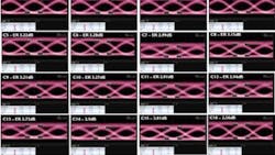
"We obtained clear and wide open eye diagrams at 56 Gbit/s non-return-to-zero on-off keying (NRZ-OOK) data rate, for all EAM and PD channels tested in a loop-back transmission experiment," says Joris Van Campenhout, director of the Optical I/O R&D program at Imec.
The GeSi EAM and PD components are available for evaluation by companies and academia through Imec's silicon photonics prototyping service and the iSiPP50G multiproject wafer (MPW) service provided by Europractice.
PROFAs and full optoelectronic packaging services are available from Chiral Photonics (OFC Booth 3714).
Source: Imec

John Wallace | Senior Technical Editor (1998-2022)
John Wallace was with Laser Focus World for nearly 25 years, retiring in late June 2022. He obtained a bachelor's degree in mechanical engineering and physics at Rutgers University and a master's in optical engineering at the University of Rochester. Before becoming an editor, John worked as an engineer at RCA, Exxon, Eastman Kodak, and GCA Corporation.
