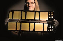
The CeGlaFlex project aims to produce wafer-thin, unbreakable, flexible ceramic and glass for displays
Mobile electronics, whether cellular phones, tablets, or blood-pressure monitors, rely on the quality of their touchscreen displays. In keeping with the trend of individually shaped smart devices, the screens should be not only scratchproof, unbreakable, and chemically stable, but they should be also easy to mold. However, this presents a dilemma for manufacturers.
"Hardened glass does not possess the required design flexibility, while malleable plastic is easily scratched," says Christian Kalupka, an ultrafast-laser researcher at Fraunhofer ILT (Aachen, Germany). "Transparent ceramics offer an alternative. Although they have the desired properties, they are not yet available in the desired sizes and lack appropriate processing methods."
This was reason enough for the Fraunhofer-Gesellschaft to initiate the internal CeGlaFlex research project (process chain for malleable ceramic and glass-based switching and display elements) in March 2017. It involves market-oriented strategic precompetitive research to develop techniques and process chains. Its objectives are to:
--manufacture thin, and as a result malleable and transparent, ceramics and display laminates
--process transparent ceramics and thin glass compounds, which can be spatially reshaped without damaging the material's functions
--produce integrated switching and display elements on malleable substrates made of ceramic-glass compounds
The MaVo project is implementing the complete process chain at five Fraunhofer Institutes. The Fraunhofer Institute for Ceramic Technologies and Systems IKTS in Dresden is developing thin, highly transparent ceramics. In Aachen, the Fraunhofer Institute for Production Technology IPT is working on processes for the precise mechanical finish (grinding and polishing) of surfaces and edges of transparent, thin ceramics and glass, while the neighboring Fraunhofer Institute for Laser Technology ILT focuses on customized laser processing (polishing, structuring, and separating). In Halle (near Leipzig), the Fraunhofer Institute for Microstructure of Materials and Systems IMWS is developing material testing methods that are important for assessing component quality. Final implementation of the process takes place at the Fraunhofer Institute for Organic Electronics, Electron Beam and Plasma Technology FEP in Dresden, which builds marketable demonstrators.
Large market potential
Kalupka is optimistic about the project’s future. "Thanks to the technologies developed in the joint project, wafer-thin ceramic will be used to manufacture flexible and unbreakable displays for portable electronics of the future," he says. "I'm confident that they will play a major role in the success of many smart mobile devices."
Source: http://www.ilt.fraunhofer.de/en/press/press-releases/PR2017/press-release-2017-4-24.html

John Wallace | Senior Technical Editor (1998-2022)
John Wallace was with Laser Focus World for nearly 25 years, retiring in late June 2022. He obtained a bachelor's degree in mechanical engineering and physics at Rutgers University and a master's in optical engineering at the University of Rochester. Before becoming an editor, John worked as an engineer at RCA, Exxon, Eastman Kodak, and GCA Corporation.
