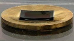
Spherically curved CMOS array improves image quality across the field
For developers of silicon-based sensor arrays such as CCD and CMOS sensors, which are all flat, the creation of a two-dimensionally curved sensor array has seemed like a close-to-impossible dream for most. A spherically curved array could be used to create a camera that could image at very high quality from center to edge of the field and at the same time simplify the camera lens design.
However, the process of photolithography needed to create a CMOS or CCD sensor requires the use of a very flat silicon wafer as a start. (If, say, a ground-and-polished concave silicon surface were used as a starting point, the lithographic process -- which has a very shallow depth of field -- used to create the array would not be able to handle the large field depth required.) Thus the end sensor result is also flat.
But some companies have created slightly spherically curved sensor arrays by bending an already-made array to a spherical shape. For example, Sony has developed a bending machine that creates slightly spherically curved CMOS arrays. In addition, Andanta GmbH (Olching, Germany) has pulled CCD arrays into a slightly spherical shape using a vacuum.
Microsoft improves the process
Now, researchers from Microsoft Research and research-and-development laboratory HRL Laboratories have developed a new method that can create image sensors with three times more spherical curvature than reported previously. They have been able to incorporate one of the sensors into a prototype camera. Compared to today’s high-end commercial single-lens reflex camera (SLR) cameras, the camera with the new sensor produced higher resolution images across the entire field of view.1
"Although the benefits of using curved sensors have been known for some time, our work now makes it practical to create cameras with curved sensors," says Richard Stoakley, a member of the research team. "Adding spherical curvature to an off-the-shelf image sensor can be done for a reasonable cost and in a way that shows significant benefits."
To make curved sensors, the researchers placed individual sensors cut from a thinned CMOS image-sensor wafer into custom-made molds and then used pneumatic pressure to push each sensor down into the mold. Other attempts at curving a sensor have typically involved gluing the edges down and trying to push on the center of the sensor. However, this creates points of high stress that cause the sensor to shatter before it reaches the target level of curvature.
The researchers coaxed significantly more curvature out of the sensors by letting them float freely during the bending process, which allowed stresses to dissipate gradually. They also used a specially shaped mold that very slowly builds stress around the chip's edges as it is pressed into the mold. Microsoft contracted HRL Laboratories, which has semiconductor fabrication capabilities and equipment, to help solve some of the specific physics challenges involved in bending the sensors.
Tests showed that curving the sensors did not change any of their electrical or imaging characteristics. When used in a prototype camera with a specially designed f/1.2 lens, a curved sensor exhibited a resolution more than double that of a high-end SLR camera with a similar lens. Toward the edges of the image, the curved sensor was about five times sharper than the SLR camera.
Although most cameras exhibit decreased light detection around the corners of the imaging sensor, the researchers showed that the curved sensors lost almost no light. This was a significant improvement compared to the decrease of around 90% measured for the commercial SLR camera.
Curved sensors for mobile phones
Although the prototype camera reported in the paper is about the size of a small consumer camera, the researchers say that the lenses could be made small enough for mobile phones and tablets. It should also be possible to build machines that could mass produce these curved sensors, allowing the additional processing to be incorporated into existing sensor manufacturing in a way that would amortize well in volume production.
The researchers are now working to see if further improvements might produce sensors with even more curvature. They also want to experiment with curving sensors that operate in infrared wavelengths, which could be useful for telescopes, 3D spatial mapping, biometric authentication, and various scientific applications. Although they caution that it is unlikely that commercial products featuring the curved sensors will be available soon, they are interested in working with other companies to further improve the sensors and to perform the strenuous robustness testing that would be needed to prepare for mass production.
REFERENCE:
1. B. Guenter et al., Optics Express (2017); doi: 10.1364/OE.25.013010
About the Author
John Wallace
Senior Technical Editor (1998-2022)
John Wallace was with Laser Focus World for nearly 25 years, retiring in late June 2022. He obtained a bachelor's degree in mechanical engineering and physics at Rutgers University and a master's in optical engineering at the University of Rochester. Before becoming an editor, John worked as an engineer at RCA, Exxon, Eastman Kodak, and GCA Corporation.

