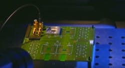
IBM engineers create low-power 60 Gbit/s optical receivers for datacenter interconnections (with video)
At the 2017 Symposia on VSLI Technology and Circuits in Kyoto Japan, researchers from IBM (Armonk, NY) unveiled an inexpensive 60 Gbit/s optical receiver intended for use in datacenters. As described by IBM electrical engineer Alessandro Cevrero, the receivers will help enable optical interconnection from processor to processor, processor to memory, from drawer to drawer inside a rack, and from a rack to a tier-1 switch.
Consuming little power, this optical receiver has the potential to replace 56 Gbit/s copper interconnects. In addition, a matching optical transmitter is expected to follow sometime next year. The two devices will complement each other to form a complete optical-receiver built in CMOS and promises to be more cost efficient than the standard copper interconnects.
“To be exact, we’re developing a single lane 60 Gbit/s optical receiver with non-return-to-zero (NRZ) signaling, targeting low cost multi-mode vertical-cavity surface-emitting laser (VCSEL) based links,” says Cevrero. “Designed in 14 nm CMOS finFET (fin field-effect transistor), the receiver features low power implementation with high jitter tolerance enabled by digital clock and data recovery.”
According to Cevrero, all interconnects greater than 1 m in length will eventually be converted from electrical to optical, which is more energy efficient and provides much more bandwidth.
“Unlike optical links, electrical links require complex equalization for high data volumes and hence, consume more power,” says Cevrero. “Our technology beats the competition as its power usage is way lower—120 mW for the receiver and eventually 300 mW for the full transceiver. What’s more, the cable length for our optical solution spans up to 100 m—a huge difference to the limited two meters electrical links offer.”
Implementing the entire 60 Gbit/s receiver on a small CMOS die doubles the transmission speed, notes Cevrero, essentially cutting the cost per gigabit per second in half. “Basically, our work demonstrates that a CMOS can achieve good optical sensitivity at data rates above 32 Gbit/s at much lower power consumption than a SiGe [silicon germanium] solution, for example,” he says. “This breakthrough CMOS photonics technology allows for closer proximity to the processor or switch chip, which provides superior sensitivity (-9 decibel-milliwatts), enables high bandwidth connectivity, and is ideal for the high throughput requirements of cloud computing.”
As the signal to the receiver is rather weak, the biggest challenge is to amplify the signal without corrupting the information, he adds.” To pull this off, we need to make sure that we can transfer data reliably,” explains Cevrero. “This requires achieving a bit error rate (BER) of 10-12, which essentially means that when transmitting 1012 bits, only one could be incorrect. At this level, we would be able to deploy our receivers in a real data center.”
Cevrero says that he and his team are currently working on a prototype targeting above 70 Gbit/s. They have also already manufactured an optical transmitter, for which measurements are expected to start in the fourth quarter of this year (2017).
Source: https://www.ibm.com/blogs/research/2017/07/low-power-high-performance-optical-receivers/

John Wallace | Senior Technical Editor (1998-2022)
John Wallace was with Laser Focus World for nearly 25 years, retiring in late June 2022. He obtained a bachelor's degree in mechanical engineering and physics at Rutgers University and a master's in optical engineering at the University of Rochester. Before becoming an editor, John worked as an engineer at RCA, Exxon, Eastman Kodak, and GCA Corporation.
