Nanoscribe’s optical 3D printers fabricate myriad types of micro-optics
Nanoscribe (Eggenstein-Leopoldshafen, Germany) has created high-precision 3D printers for fabrication of micro-optical components. Using Nanoscribe´s 3D printer Photonic Professional GT, which is based on two-photon polymerization, a broad range of almost arbitrary micro-optical shapes, including standard refractive micro-optics, freeform optics, diffractive optical elements, and even multiplet lens systems can now be printed in a one-step process.
The additive-manufacturing process used is, of course, very different from the conventional grinding and polishing of lenses; advantages include a great reduction in geometrical constraints and easy, fast (within a few days) production of one to many elements. Nanoscribe says that the process produces high shape accuracy and optically smooth surfaces.
And another very interesting feature: photonic "wirebonds" can be fabricated using the same 3D printing technology in the same production process. A photonic wirebond is basically a fabricated-in-place optical fiber that can be used to duct light from one optic to another, one optoelectronic component to another, or even one photonic chip to another.
Here are a few examples of components 3D-printed with Nanoscribe’s process:
Foveated imaging
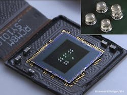
Researchers from the University of Stuttgart used a Photonic Professional GT system to print micro-objective lenses with different focal lengths onto a high-resolution CMOS chip. All images created by the lenses on the chip are simultaneously read out electronically and processed into an image with a significantly improved resolution in the center. This so-called "foveated imaging" is attractive for the production of cameras with sensors that mirror the extra wide field of vision of an eagle´s eye—for example, for applications in the automotive or smartphone industry as well as in the medical field.
Array of micro-optic hemispheres
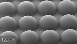
This array of hemispheres demonstrates the high shape accuracy and optically smooth surfaces achievable by using two-photon polymerization. The printed hemispherical microlenses have a shape accuracy better than 1 µm and a surface roughness better than 10 nm Ra. The array with a size of 1 square centimeter in total and hemispheres with a height of 150 µm was written into a solid negative-tone resist. Due to the optimized combination of hardware and software components, a high and consistent precision is achieved across the entire writing field.Diffractive optical elements
Using a Nanoscribe system, the fabrication of diffractive optical elements (DOEs), which typically have significantly smaller feature sizes than refractive optics, is possible as well. DOEs can be designed for functionalities that are hardly accessible with refractive optics, such as the generation of almost arbitrary light distributions in the far-field. Using a Photonic Professional GT 3D printer, functional multilayered diffractive optical elements can be directly patterned onto glass substrates enabling rapid prototyping and design iterations within a few days.Nickel shims for optics mass production
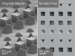
The challenge of fast and low-cost production of micro-optical elements can be solved by fabricating a nickel shim from the printed polymer structures by electroforming, allowing standard replication techniques such as injection molding or hot embossing to be used for subsequent mass replication. Replication using nanoimprinting is another viable route.
John Wallace | Senior Technical Editor (1998-2022)
John Wallace was with Laser Focus World for nearly 25 years, retiring in late June 2022. He obtained a bachelor's degree in mechanical engineering and physics at Rutgers University and a master's in optical engineering at the University of Rochester. Before becoming an editor, John worked as an engineer at RCA, Exxon, Eastman Kodak, and GCA Corporation.


