Electrically pumped quantum-dot near-IR microlaser on silicon has submilliamp threshold
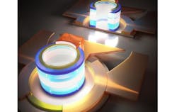
Researchers from the Hong Kong University of Science and Technology (HKUST) and the University of California, Santa Barbara (UCSB) have now created record-small electrically pumped microlasers epitaxially grown on industry-standard (001) silicon (Si) substrates.1 The devices operate in a whispering-gallery-mode microlaser with a radius of 5 μm, have a submilliamp threshold of 0.6 mA, emit in the near-IR (1.3 μm), and operate at temperatures up to 100 °C. The thresholds and footprints are orders of magnitude smaller than those previously reported lasers epitaxially grown on Si, say the researchers.
It should be noted that a somewhat similar development was reported in 2016 by a group of researchers from University College London (London, England), the University of Sheffield (Sheffield, England), and Cardiff University (Cardiff, Wales).
III-V devices
The gallium arsenide (GaAs) based III-V semiconductor devices from HKURST and UCSB, which also incorporate aluminum (Al) and indium (In), consist of a GaAs layer on Si, 15 periods of thin (5 nm/5 nm) Al0.3Ga0.7As/GaAs layers, and seven InAs/InGaAs quantum dot-in-a-well layers in the laser's active region.
"The realization of high-performance micron-sized lasers directly grown on Si represents a major step toward utilization of direct III-V/Si epitaxy as an alternate option to wafer-bonding techniques as on-chip silicon light sources with dense integration and low power consumption," says Kei May Lau, a professor at HKUST.
From optical to electrical pumping
The two groups had previously developed optically-pumped continuous-wave (CW) microlasers operating at room temperature that were epitaxially grown on silicon with no germanium buffer layer or substrate miscut. "Electrical injection of microlasers is a much more challenging and daunting task: first, electrode metallization is limited by the micro-sized cavity, which may increase the device resistance and thermal impedance; second, the whispering gallery mode (WGM) is sensitive to any process imperfection, which may increase the optical loss," says Yating Wan, a HKUST PhD graduate who is now at UCSB.
"As a promising integration platform, silicon photonics needs on-chip laser sources that dramatically improve capability while trimming size and power dissipation in a cost-effective way for volume manufacturability," says John Bowers, deputy chief executive officer of AIM Photonics (Rochester, NY), a consortium devoted to developing the U.S integrated photonics industry. "The realization of high-performance micron-sized lasers directly grown on Si represents a major step toward utilization of direct III-V/Si epitaxy as an alternate option to wafer-bonding techniques."
Source: https://eurekalert.org/pub_releases/2017-09/hkuo-sd1091817.php
REFERENCE:
1. Yating Wan et al., Optics (2017); https://doi.org/10.1364/OPTICA.4.000940
About the Author
John Wallace
Senior Technical Editor (1998-2022)
John Wallace was with Laser Focus World for nearly 25 years, retiring in late June 2022. He obtained a bachelor's degree in mechanical engineering and physics at Rutgers University and a master's in optical engineering at the University of Rochester. Before becoming an editor, John worked as an engineer at RCA, Exxon, Eastman Kodak, and GCA Corporation.

