Berkeley Lab and aBeam develop process to nanoimprint devices on tip of an optical fiber
A high-throughput fabrication technique allows researchers to print a nanoscale imaging probe and potentially other devices onto the tip of a glass optical fiber. The process opens the door for the widespread adoption of this and other nano-optical structures that squeeze and manipulate light in ways that are unachievable by conventional optics. Nano-optics have the potential to be used for imaging, sensing, and spectroscopy, and could help scientists improve solar cells, design better drugs, and make faster semiconductors, but a big obstacle to the technology's commercial use has been its time-consuming production process.
The new fabrication method, called fiber nanoimprinting, could unplug this bottleneck. It was developed by scientists at the Molecular Foundry, located at the Department of Energy's Lawrence Berkeley National Laboratory (Berkeley Lab; Berkeley, CA), in partnership with scientists aBeam Technologies (Hayward, CA). Their research is reported online May 10 in the journal Scientific Reports.
RELATED ARTICLE: EV Group and Swiss Litho develop 3D nanoimprint lithography system with 1 nm accuracy
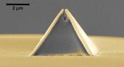
Their work builds on the Campanile probe, which was developed by Molecular Foundry scientists four years ago. Its tapered, four-sided shape resembles the top of the Campanile clock tower on UC Berkeley's campus. The probe is mounted at the end of an optical fiber, and focuses an intense beam of light onto a much smaller spot than is possible with current optics. This enables spectroscopic imaging at a resolution 100 times greater than conventional spectroscopy, which only maps the average chemical composition of a material. In contrast, the Campanile probe can image the molecule-by-molecule makeup of nanoparticles and other materials. Scientists can use it to examine a nanowire for minute defects, for example, leading to new ways to improve nanowires for use in more efficient solar cells.
"When we first made the Campanile probe, we sculpted it with an ion beam like Michelangelo. It took about a month," says Stefano Cabrini, director of the Nanofabrication Facility at the Molecular Foundry. "That pace is OK for research applications, but the lack of a mass-fabrication method has inhibited the wider use of nano-optical devices."
That's where fiber nanoimprinting comes in. Its first step is the most time consuming: Scientists create a mold with the precise dimensions of the nano-optical device they want to print. For the Campanile probe, this means a mold of the probe's nanoscale features, including the four sides and the light-emitting 70-nanometer-wide gap at the pyramid's top.
"This mold can take a few weeks to make, but we only need one, and then we can start printing," explains Keiko Munechika of aBeam Technologies, which partnered with the Molecular Foundry to develop the fabrication process as part of the Department of Energy's Small Business Technology Transfer program. Several other aBeam Technologies scientists contributed to this work, including Alexander Koshelev. The company is now commercializing various fiber-based nanooptical devices.
After the mold is created, it's off to the races. The mold is filled with a special resin and then positioned atop an optical fiber. Infrared light is sent through the fiber, which enables the scientists to measure the exact alignment of the mold in relation to the fiber. If everything checks out, UV light is sent through the fiber, which hardens the resin. A final metallization step coats the sides of the probe with gold layers. The result is a quickly printed—not meticulously sculpted—Campanile probe. The fabrication technique can also be applied to any nano-optical device, and has so far been used to create Fresnel lenses and beam splitters in addition to the Campanile probe.
SOURCE: Lawrence Berkeley National Laboratory; http://newscenter.lbl.gov/2017/05/10/print-nanoscale-imaging-probe/

Gail Overton | Senior Editor (2004-2020)
Gail has more than 30 years of engineering, marketing, product management, and editorial experience in the photonics and optical communications industry. Before joining the staff at Laser Focus World in 2004, she held many product management and product marketing roles in the fiber-optics industry, most notably at Hughes (El Segundo, CA), GTE Labs (Waltham, MA), Corning (Corning, NY), Photon Kinetics (Beaverton, OR), and Newport Corporation (Irvine, CA). During her marketing career, Gail published articles in WDM Solutions and Sensors magazine and traveled internationally to conduct product and sales training. Gail received her BS degree in physics, with an emphasis in optics, from San Diego State University in San Diego, CA in May 1986.
