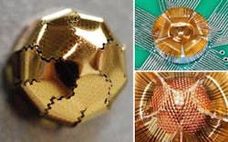
Bowl-shaped silicon image sensor could enable hemispherical imaging
While CCD and CMOS sensors are conventionally flat, they can be curved a little bit by forcing then into a concave semispherical form, then gluing them. This method produces a sensor field that can be curved enough to, for example, enable the design of simpler imaging optics.
However, far more deeply curved concave image sensors could allow more exotic devices such as small cameras that could image almost an entire hemisphere (perhaps with a monocentric lens); highly convex sensors could lead to insect-eye type imagers. But silicon simply does not stretch enough to allow forcing it into a true bowl shape.
Now, researchers from the University of Wisconsin-Madison and the University of Texas at Arlington have created a somewhat origami-like method of creating deeply bowl- or dome-shaped silicon detectors.1 It involves precise laser-cutting of a hexagonal sensor array on silicon so that the remaining array can be folded into the form of a geodesic dome (this is not true origami because origami doesn't allow cutting).
To create a curved photodetector, Zhenqiang (Jack) Ma, a professor at the University of Wisconsin-Madison, and his group formed pixels by mapping the repeating hexagons onto a thin, flat flexible sheet of silicon called a nanomembrane, which sits on a flexible substrate. They then used a laser to cut away some of those pixels so the remaining silicon formed perfect, gapless seams when they placed it atop a dome shape (for a convex detector) or into a bowl shape (for a concave detector).
The researchers' current prototype is approximately 7 mm in diameter. Although the pixel density is low, this could be vastly increased in future devices.
Source: https://news.wisc.edu/optoelectronics-origami-an-easy-to-make-double-duty-curved-image-sensor/
REFERENCE:
1. Kan Zhang et al., Nature Communications (2017); doi: 10.1038/s41467-017-01926-1

John Wallace | Senior Technical Editor (1998-2022)
John Wallace was with Laser Focus World for nearly 25 years, retiring in late June 2022. He obtained a bachelor's degree in mechanical engineering and physics at Rutgers University and a master's in optical engineering at the University of Rochester. Before becoming an editor, John worked as an engineer at RCA, Exxon, Eastman Kodak, and GCA Corporation.
