Military program develops novel UV sources

A research program at the Defense Advanced Research Projects Agency (DARPA; Arlington, VA) aims to create novel semiconductor ultraviolet optical sources (SUVOS) for use in biological-agent detection and a many other military applications.1 The motivation for the program is to enable more efficient and cost-effective fluorescence-based biosensors. Current biosensors use "large, power-hungry lasers," according to John Carrano, DARPA SUVOS program manager. One such biosensor subsystem in development at the Massachusetts Institute of Technology Lincoln Laboratory (Lexington, MA), called a biological aerosol warning system, consumes 25 W of power using the smallest ultraviolet laser available, which is sold by JDS Uniphase (JDSU; San Jose, CA).
Used in biosensor systems to detect biological agents such as anthrax, the JDSU laser is a quadrupled, solid-state, Q-switched Nd:YAG that costs about $10,000. Besides the cost, says Carrano, the problem with the existing commercially available lasers is that they limit the development of biosensors to 266- and 355-nm wavelengthsneither of which is ideal for biosensors (see figure).
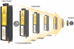
To achieve more-practical UV sources, one goal of the SUVOS program is to shrink the existing ultraviolet laser and its power supply by 500 times, to about the size of a dime. Other goals of the program are to reduce power consumption of the source to less than 100 mW, reduce weight from 4 kg to 2 g, and cut the cost to $100 per source. The program expects to deliver light-emitting devices (LEDs) for biodetection that emit at 280 nm and operate on less than 10 mW, and 340-nm laser diodes that operate on less than 25 mW.
UV-based transceiver
Another target in the SUVOS program is to develop a UV-based transceiver for covert non-line-of-sight (NLOS) optical communications. Covert communications are limited in conventional radio-frequency technology by the amount of power consumed. Based on aerosol or Rayleigh scattering, a UV optical transceiver would enable low-power, short-range squad radios that would be difficult for the enemy to detect, as well as networked unattended ground sensors.
"The short wavelength of ultraviolet energy doesn't propagate very far before scattering," says Carrano, "so it lends itself to covertness." Also promising is the development of military communications in urban settings, because UV can easily scatter around buildings. Other military applications of SUVOS include water purification, equipment and personnel decontamination, and white-light generation. In the NLOS covert communication and biosensor applications, UV LED and laser-diode semiconductor emitters at 340-nm will be available within a year, predicts Carrano.
More holes
A primary challenge to SUVOS technology is achieving sufficient p-type conductivity in high-aluminum-content III-nitride materials. In a semiconductor injection device, a diode works via a positively charged (p-type) material that supplies charge-carrying "holes" and a negatively charged (n-type) material consisting of electrons. The two materials are sandwiched together by simply growing one on top of the other. A positive voltage applied to the p-side and a negative voltage to the n-side causes the electrons and holes to recombine radiatively to produce photons. The answer to an insufficient number of holes for p-type doping activation may be an infrared pump to ionize electrons and create more holes, says Carrano.
Director of external affairs at DARPA, Jan Walker, says the SUVOS program is expected to cost $45 million over four years, depending on yearly congressional appropriations. Phase I of the SUVOS program, a two-year effort, will concentrate on the development of suitable UV photonic materials by exploiting the unique characteristics of wide-bandgap semiconductors. Also included in the Phase I effort is the design and fabrication of innovative optoelectronic device structures operating in the UV.
Effectively begun in October 2001, the program is currently in contract negotiations, says Walker. A primary contract for $14.5 million over four years has been awarded to Cree (Durham, NC), which accordingly has designated University of California Santa Barbara and North Carolina State University as subcontractors, both affiliated with Cree and undertaking the development of blue LEDs.
REFERENCES
1. John C. Carrano et al, SPIE AeroSense (April 2002).
2. Shuji Nakamura, The Blue Laser Diode, Springer (1997).

Valerie Coffey-Rosich | Contributing Editor
Valerie Coffey-Rosich is a freelance science and technology writer and editor and a contributing editor for Laser Focus World; she previously served as an Associate Technical Editor (2000-2003) and a Senior Technical Editor (2007-2008) for Laser Focus World.
Valerie holds a BS in physics from the University of Nevada, Reno, and an MA in astronomy from Boston University. She specializes in editing and writing about optics, photonics, astronomy, and physics in academic, reference, and business-to-business publications. In addition to Laser Focus World, her work has appeared online and in print for clients such as the American Institute of Physics, American Heritage Dictionary, BioPhotonics, Encyclopedia Britannica, EuroPhotonics, the Optical Society of America, Photonics Focus, Photonics Spectra, Sky & Telescope, and many others. She is based in Palm Springs, California.