MICROBOLOMETERS: One-mil uncooled array has low noise and high fill factor
CHUAN LI and PHILLIP HOWARD
Performance improvements in vanadium oxide (VOx) microbolometer arrays have stirred interest for insertion into military systems that require low-cost large-format, high-sensitivity detectors. Smaller pixel pitch further benefits some of these applications by reducing the optics size and weight, decreasing the array production cost, and simplifying package form factors. As the size of the detector is reduced, however, the energy collected scales to the area of the detector, and higher thermal isolation and increased detector fill factor are required to maintain sensitivity. As result, there is a delicate tradeoff between the requirements for sensitivity versus smaller detector size. Recently, enhancements in the thermal-isolation structures and small pixel configuration have allowed demonstrations of 1‑mil (25.4-µm pixel size) pixel arrays with less than 30‑mK noise-equivalent temperature difference (NETD).
These arrays are finding broader use in military systems. DRS has received two contracts to build thermal-weapon-sight and driver’s-viewer-enhancer systems using large-area uncooled focal-plane arrays. The specifications call for 1-mil 640 × 480 and 320 × 480 arrays that operate over the -40°C to 65°C range. These requirements can be met by newly developed microbolometer arrays.
Focal-plane-array designs
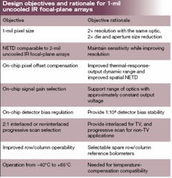
The high density 1-mil-pixel-size 640 × 480 uncooled IR focal-plane arrays can provide doubled spatial resolution with the same sensor envelope and optics as older 2-mil (50.8‑µm) 320 × 240 arrays (see table). They were also designed to provide significantly reduced camera size, weight, and cost, and provide NETD performance comparable to that of the larger 2-mil pixel size.
The 1-mil arrays include advanced design features that have been demonstrated on the 2-mil pixel size. The designs incorporate a parallel “smart-sensor” data bus, which controls the focal-plane operation and provides pixel offset compensation data from sensor electronics. Both designs include precision on-chip temperature measurements over the entire camera operating temperature range that is streamed onto the video-output channel during horizontal blanking.
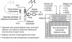
The design concept for the interface between the bolometer and the readout-integrated-circuit (ROIC) interface is embodied in both designs (see Fig. 1). It is essentially a Wheatstone-bridge network, which is very effective in eliminating the detector bias offset and any bias supply noise by common-mode rejection in the network’s differential output. Bias supply noise includes the detector’s bias-induced transient-heating effect, which generates a significant output voltage change on each leg of the bolometer bridge network during each bias pulse. The differential output voltage of the bridge network is applied to a transimpedance amplifier that converts the voltage difference into a current, which is integrated to form the final pixel-signal voltage that is then sampled and multiplexed.
One or more heatsinked bolometers are located at one end of each array column, and one or more optically shielded reference detector bolometers are located at one end of each detector-array row. A set of analog electronics, consisting of a transconductance amplifier, a signal integrator network, and a sample-and-hold network, is located at one end of each detector-array column. In operation, when a row is selected for bolometer resistance sensing, a voltage bias pulse is applied in parallel to all bolometers in the selected row to sense the bolometer resistance values. The optically shielded reference bolometer at the end of the selected row is then shared by all detectors in the row during resistance sensing. Pixel-array readout, as a result, is ripple mode.
Microbolometer structure
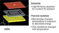
The basic structure adopted for the 1‑mil microbridge can be broken down into three layers (see Fig. 2). At the bottom of the structure, is the ROIC. The success of the uncooled IR focal-plane arrays relies heavily on the ability to read out small signals from the microbridge with introduction of minimal noise.
The second layer in this structure is the thermal-isolation structure (TIS). At the center of this layer is the VOx thin film that detects a change in resistance as the microbridge is heated from the incident radiation. The thermal isolation is provided by two connecting “legs” to the ROIC substrate. These provide the electrical connections to the readout and the mechanical support to suspend the VOx layer. A large portion of the space in the thermal-isolation structure is taken up by the legs, leaving a relatively small area for VOx. In a typical single-layer microbridge, this area is responsible for absorption of the IR radiation; designs attempt to maximize this area by decreasing linewidth and line spacing in the microbridge structure.
A patented top layer in the microbridge structure, called the “umbrella” layer, is added to enhance absorption while relaxing the photolithographic requirements in the thermal-isolation structure. With a single post for thermal contact to VOx, the umbrella extends up from the center of the VOx and fans out to cover more than 95% of the pixel. The structure consists of absorbing dielectric films that work in concert with the underlying thermal-isolation structure to absorb the incident IR radiation. Because the reflectivity and the gap height vary under this umbrella, the absorptivity varies across the pixel. Absorptivity is calculated for each area of the pixel and summed to determine the effective absorptivity. Our calculation for this three-layer structure estimated an absorption efficiency of 75% over the 8- to 12-µm range, compared with 52% without an umbrella layer.
Small-pixel performance
Illustrative examples of imagery were obtained for the 640 × 480 uncooled IR focal-plane array (see Fig. 3). An image photo from the initial ROIC design shows a perceptible level of columnar pattern noise in the image that was caused by higher than expected metal-oxide semiconductor field-effect transister (MOSFET) 1/f noise from the ROIC. Imagery was also obtained after the ROIC design was modified to reduce the effective level of ROIC 1/f noise and the oxide-umbrella pixel design tweaked to optimize overall performance. In this case, the columnar noise is no longer perceptible, and the F/1 NETD is less than 30 mK under conditions that are compatible with uncooled IR focal-plane-array sensor operation when operating in the temperature-compensating mode developed at DRS.
The 1-mil readout circuit uses a temperature-compensating design to compensate for thermal drift that can lead to fixed pattern noise. This design, combined with array uniformity, has enabled us to operate the devices at ambient temperature without using thermoelectric coolers.
Chuan Li is engineering director at DRS Infrared Technologies, Nytech Imaging Systems, 14450 Myford Rd., Irvine, CA 92606; Phillip Howard is senior technologist at DRS Sensors and Targeting Systems, 10600 Valley View Street, Cypress, CA 90630; e-mail: [email protected]; www.drsinfrared.com.


