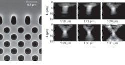
Negative refraction and focusing of millimeter waves by dielectric-rod-type or air-hole-type 2-D photonic crystals (PCs) has been demonstrated; however, focusing light waves is more difficult due to observed weak optical confinement and unwanted reflection/diffraction of light waves in a PC structure. Recognizing that a high-index-contrast PC slab using a silicon-on-insulator (SOI) substrate can enhance optical confinement (despite increasing diffraction and reflection losses), researchers at Yokohama National University (Yokohama, Japan) used finite-difference time-domain (FDTD) simulations to model an optimum interface that reduces these losses and successfully fabricated the structure to demonstrate focusing of 1.26 to 1.42 µm light by negative refraction.1
Deformed air holes
The SOI substrate consisted of 0.26-µm-thick silicon (Si) and 1.0-µm-thick silicon dioxide (SiO2) layers. Device patterns were formed using electron-beam lithography and plasma etching, and the air-bridge PC structure was formed using hydrofluoric wet etching. The PC structure consists of air holes in a square lattice rotated by 45°, with a linear array of deformed air holes just at the SOI boundary that reduces optical reflection and diffraction (see figure). The deformed air holes have a round front shape and a triangular back shape. The FDTD simulations dictated that, for negative refraction to occur in the superlens, the air-hole diameter normalized by the PC lattice constant should equal 0.689 and the effective refractive index of the PC slab should be 2.963 (the lattice constant is 0.45 µm).
To demonstrate focusing by the fabricated superlens, a silicon-wire waveguide with 0.5 µm width was used as the source of the Gaussian input to the superlens. The fabrication of the wire waveguide included mode expanders to ensure smooth light transmission. The waveguide was connected to a 77-µm-long Si slab and the full-width at half-maximum of the Gaussian beam (after exiting the wire and traveling through the Si slab) was around 13 µm at the input end of the superlens to satisfy another FDTD requirement that the divergence of the angle of incident light to the superlens be within 12° for negative refraction to occur.
To study the focusing effect over a range of wavelengths, a tunable laser source was used to deliver light to the wire waveguide and through the Si slab to the superlens. For wavelengths between 1.26 and 1.31 µm, focusing was clearly observed within the superlens through direct observation of radiated light in the near-field pattern within the superlens. For longer wavelengths beyond 1.31 µm, smaller angular components are not as easily observed and require more-complex methods; however, focusing was observed over a wavelength range from 1.26 to 1.42 µm. Comparison between FDTD simulations and experimental results was favorable.
The superlens fabricated by the researchers can produce a minimum focused-spot width of 1.8 µm. “The superlens is unique because it forms a real image by its flat surface and its lensing characteristics are independent of light input position,” says researcher Toshihiko Baba. “It has the potential of changing the design rules for optical couplers and imaging systems. We are now planning to demonstrate the position-independent focusing characteristics and some unique components based on this lens, such as optical cavities and waveguides.”
REFERENCE
1. T. Matsumoto et al., Optics Lett. 31(18) 2786 (Sept. 15, 2006).

Gail Overton | Senior Editor (2004-2020)
Gail has more than 30 years of engineering, marketing, product management, and editorial experience in the photonics and optical communications industry. Before joining the staff at Laser Focus World in 2004, she held many product management and product marketing roles in the fiber-optics industry, most notably at Hughes (El Segundo, CA), GTE Labs (Waltham, MA), Corning (Corning, NY), Photon Kinetics (Beaverton, OR), and Newport Corporation (Irvine, CA). During her marketing career, Gail published articles in WDM Solutions and Sensors magazine and traveled internationally to conduct product and sales training. Gail received her BS degree in physics, with an emphasis in optics, from San Diego State University in San Diego, CA in May 1986.
