MICROSCOPY: Differential-polarization technique enables precise 3-D nanoimaging
A reflective optical arrangement that allows control of the properties of polarized light has enabled development of an optical-imaging technique for precise 3-D thickness, dimensional, roughness, profile and step-height measurements at the nanometer scale. The technique—developed by engineers at Nano-lane (Montfort-le-Gesnois, France), distributed by Microphotonics (Irvine, CA) in North America, and dubbed Sarfus—increases the axial sensitivity of an optical microscope by about two orders of magnitude without reducing lateral resolution. It is intended for applications such as static and dynamic visualization of items such as ultrathin films, nanotubes, and nanowires.
Sarfus visualization results from a significant increase of optical-microscope sensitivity, achieved by enhancing the contrast of the object in relation to its background, provided in this method by a contrast-enhancing sample-supporting plate referred to as a “surf.” Surfs can be used in either air or liquid environments; their specific optical properties can be manipulated by customizing the layers deposited on the substrate with specific top-layer materials such as silicon dioxide, gold, chromium, or aluminum. When a beam of white light is passed through a linear polarizer prior to hitting the sample mounted on the surf, the sample induces a change in the polarization state but the surf does not. So when the reflected light passes through an analyzer crossed with the polarizer, the light reflected from the surf is stopped, whereas the light reflected from the sample passes through.
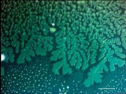
The resulting high-contrast images allow direct observation and measurement of nanoscale film thicknesses or nanoscale object and feature dimensions, as in this copolymer crystallization. Two-dimensional images can also be converted into precise 3-D metrological images with spatial resolution below 1 nm. Roughness, profile extraction, and step-height measurements can be imaged as well. Contrast on standard surf sample supports exceeds that of silicon wafer materials by a factor of 25 for ultrathin film samples of 10 nm thickness, and by a factor of 160 for a sample of 1 nm thickness.
Current and potential applications include biomedical studies such as rapid defect visualization for soft lithography, real-time visualization and dynamic study of phospholipids, and quality control and thickness-measurement determination of DNA biochips. Thin films and surface-treatment studies include characterizing layer homogeneity of organic steps, direct visualization and height-deposition measurements of plasma, dynamic studies of crystallization and wetting applications, direct behavior and morphology characterization of nanotubes and nanowires, and direct visualization of nanolithography patterns with quality control of the deposition process.
Hassaun A. Jones-Bey | Senior Editor and Freelance Writer
Hassaun A. Jones-Bey was a senior editor and then freelance writer for Laser Focus World.
