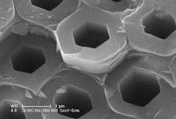
A team from Penn State University (State College, PA) and the University of Southampton (Southampton, England) has demonstrated a hybrid semiconductor and optical-fiber technology in which semiconductor devices were grown inside microstructured optical fibers (MOFs). Advantages include the fact that the light does not have to leave the fiber to interact with the electronic devices, and that the devices can interact with the light over a long distance within the fiber, making use of effects that would not otherwise be strong enough to be useful. The researchers expect the new technology to have applications in fields as diverse as communications, medicine, computing, and remote-sensing devices.
The new technique allows optical fibers to be constructed, and the functional materials to be chemically deposited in distinct and independent steps, giving the full design flexibilities of both platforms. The fibers are made in the usual way, by stacking and fusing arrays of capillaries into preforms centimeters in diameter that are then drawn into fibers at high temperature. Careful design of the stacked preform allows the capillary holes within a single MOF to have a wide range of shapes and sizes, in both periodic and aperiodic spatial configurations. The generally preferred method for depositing semiconductors and metals is chemical vapor deposition (CVD). However, depositing via CVD onto the walls of the long, extremely narrow pores in a MOF presents challenges in terms controlling the deposition and the mass transport of reactants into, and byproducts out of, such a confined space.
Depositing semiconductors in voids
In this work, high-quality polycrystalline and single-crystal semiconductors are deposited within the voids of MOFs by using high-pressure microfluidic chemical deposition. The high-pressure flow is possible because of the very high mechanical strength of optical fibers, and it overcomes mass-transport constraints, producing what the team claims is a “strikingly uniform, dense, and conformal annular deposition” onto the capillary walls, even for pores that reduce to less than 10 nm in diameter.
In a typical experiment, a germanium-containing gas flows through the heated MOF at a partial pressure of 2 MPa, along with an inert carrier gas. A smooth layer of amorphous germanium begins to deposit on the pore walls as the temperature is ramped up past 300°C. Crystalline grains then nucleate and grow as the temperature exceeds the crystallization point of 375°C. A uniform tube forms, and a 1.0 µm diameter pore can be narrowed by a factor of 100 (down to 25 nm or smaller), tapering open gradually over a deposition length of 70 cm. The group reported that silica capillaries drawn to a 100 nm diameter were also successfully filled with germanium to form nanotubes over lengths of up to 30 cm, with an inner diameter of less than 10 nm.
Transistor inside a fiber
To demonstrate that electrically active germanium has been deposited into optical fibers over macroscopic lengths, the team fabricated an 11 mm long, 5 mm diameter field-effect transistor (FET) inside a single silica capillary of 94 mm outer diameter. Operation of the FET was then characterized electrically.
Silicon has been deposited in a manner similar to that of germanium (see figure). It is also possible to produce fiber-integrated compound semiconductors, semiconductor heterostructures, and metal semiconductor heterostructures. The team claims to have integrated annular layers of mid-infrared transparent germanium sulfide, coaxial silicon-germanium heterojunctions, and annular gold/silicon Schottky junctions into MOFs by sequential deposition. In addition, the high transparency of the MOF templates has allowed the team to put thermally sensitive or photosensitive precursors along the fiber axis and pattern in all three spatial dimensions.“If we can actually generate signals inside a fiber, a whole range of optoelectronic applications becomes possible,” says John Badding, a Penn State researcher. “For example, in endoscopic surgery, by building a laser inside the fiber you might be able to deliver a wavelength that could not otherwise be used.”
The new technology offers an opportunity to build hybrid devices that will perform light generation, detection, manipulation, and switching functions faster and more effectively than before.
“So far, the team has demonstrated a transistor inside a fiber using this technique, but other optoelectronic devices like diode lasers could mean a fundamental advance in the way optical communications works,” says Pier Sazio, from the Optoelectronics Research Centre in the University of Southampton.
Bridget Marx | Contributing Editor, UK
Bridget Marx was Contributing Editor, UK for Laser Focus World.

