PHOTONIC CRYSTALS: Demultiplexers harness photonic-crystal dispersion properties
Three dispersive properties of photonic crystals-the superprism effect, negative diffraction, and negative refraction-were used in combination to produce the most compact photonic-crystal demultiplexer to date.
BABAK MOMENI AND ALI ADIBI
The idea of photonic crystals (PCs) as synthetic optical materials with “controllable” properties has been advanced by progress in photonic-crystal fabrication technologies and improvements in the conceptual understanding of their properties. Besides applications that utilize their photonic bandgap mainly for light confinement, PCs can also be exploited to harness their unique dispersive properties.1, 2, 3 Of particular interest is the ability of PCs to perform parallel demultiplexing in a very small footprint that is compatible with chip-scale integrated photonic circuits.
In addition to applications in optical communications, compact optical wavelength-demultiplexing (WD) devices have received increasing attention as building blocks for spectral analysis in “lab-on-a-chip” biosensing applications and integrated optical circuits for optical information processing. These compact WD devices are used to separate several optical channels at different wavelengths with high spectral resolution (separation of channels with small wavelength difference between adjacent channels), and low crosstalk (negligible presence of unwanted channels at the location of the desired channel).
Despite these application demands, compact WD devices with the required properties for practical applications have not yet been realized because of the lack of an appropriate optical material with high dispersive properties to allow for the formation of compact structures on a chip. But recent advances in dispersion engineering using PCs may be changing this reality.
Designing a high-resolution demultiplexer
To realize an efficient spectrometer, in addition to a compact WD mechanism to achieve spatial separation of different wavelength channels, special measures must be taken to achieve high isolation from unwanted wavelength channels.
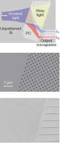
The basic demultiplexing function can be obtained using the superprism effect in PCs (see Fig. 1).4, 5 For wavelength demultiplexing, the superprism effect is based on the difference between the dispersive properties of the PC and the incident region, which causes different wavelength channels inside the PC region to propagate in different directions (determined by the direction of group velocity of the corresponding PC mode at each wavelength). Although propagation in such a medium can eventually result in separation of different wavelength channels, it has been shown that the diffraction of the optical beam at each wavelength channel results in broadening of the beam and requires relatively large propagation length to achieve spatial separation with the required crosstalk level between adjacent channels. Because the resolution of this conventional configuration is limited, these demultiplexers are not suited for high-resolution applications.6, 7
Research at the Georgia Institute of Technology (Atlanta, GA), however, supports the development of compact, high-resolution demultiplexers by combining two dispersive properties of PCs: the superprism effect and negative diffraction.8, 9, 10 In these structures, the broadening of the beam due to normal diffraction effects is compensated by propagation in a PC region with negative diffraction. As a result of such diffraction compensation, the size of the beam at the output of these structures is reduced to approximately the transfer-limited beamwidth, requiring a much smaller propagation length for spatial separation of adjacent wavelength channels. Another unique property of PCs is the negative refraction at their interface. In this case, the desired signal is refracted away from the direction of the incident signal, resulting in the separation of the desired signal from the stray signals. By combining the superprism effect and negative diffraction with negative refraction of the desired signals, the crosstalk in the PC demultiplexers can be further reduced.
It is possible to combine several unique dispersive properties of PCs for a desired application by optimizing the PC geometry (the size and periodicity of the holes) for the frequency range of interest.10 By such optimal dispersion engineering in PC devices, it is possible to simultaneously focus the separated channels down to a small size while propagating through the PC and divert the separated channels from the stray and unwanted signals. These considerable improvements are obtained without adding to the complexity of fabrication or requiring any special material growth processes.
Implementation
Using the design techniques just described, we constructed a PC device for superprism demultiplexing in the form of a slab-type planar structure with two-dimensional in-plane periodicity by using the recently developed effective-index technique (see Fig. 2).11 Light incident on the PC region comes from an unpatterned silicon region and the output light goes through an array of 5 µm wide output waveguides (1 µm distance between neighboring waveguides). Each output waveguide is tapered down to 2 µm at the output end of the devices. The waveguide array has been designed to observe the output of the PC structure with a reasonable spatial resolution. Each separated wavelength channel corresponds to two output waveguides to observe the possible crosstalk between adjacent channels more clearly.
The PC structure was fabricated on a silicon-on-insulator (SOI) wafer with a 3 µm silicon oxide layer sandwiched between a thick silicon (Si) substrate and a 220 nm layer of Si (on top), and covered by 50 nm of silicon-oxide that is used as a hard-mask during the fabrication process. We used electron-beam lithography and inductively coupled plasma (ICP) etching to generate the two-dimensional periodic pattern in the thin Si layer.
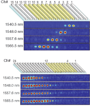
In the measurement setup, light from a tunable laser is end-coupled into the input Si region through a conventional dielectric ridge waveguide. The output edge of the device is imaged onto an IR camera to record the results (see Fig. 3). Measured results show clear spatial separation of the wavelength channels and desired small spot size from diffraction compensation. Also by designing the device in the negative refraction regime for TE-like polarization, the unwanted polarization (TM) is successfully isolated from the desired signals.
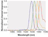
To characterize our designed PC demultiplexer more quantitatively, the output from each waveguide is isolated and its power is measured using an IR detector connected to a lock-in amplifier (see Fig. 4). Four channels are separated in this device with a wavelength spacing of 8 nm, and channel isolations (the power in the desired channel divided by the sum of contributions of other channels at the location of the desired one) are better than 6.5 dB.10 This integrated superprism-based demultiplexing device has a PC area of less than 50 x 100 µm, two orders of magnitude smaller than other experimental demonstrations of superprism-based PC demultiplexers using conventional geometry (scaled to the same performance) reported to date. Using the same scheme, a 64-channel demultiplexer with channel spacing of 0.5 nm can be realized in a 4 mm2 PC structure. To the best of our knowledge, this is the best overall performance for a PC demultiplexer reported to date.
null
Outlook
The possibility of combining several functionalities including the superprism effect, negative refraction, and negative diffraction, brings a new dimension into the design approach for “synthetic” optical materials. With maturing fabrication technology and further improvements in device design, even better performances are expected in the near future.
ACKNOWLEDGMENT
This work was supported by the Air Force Office of Scientific Research under Contract No. F49620-03-1-0362 (G. Pomrenke) and by the National Science Foundation under Contract No. ECS-0239355 (L. Goldberg).
REFERENCES
1. E. Yablonovitch, Phys. Rev. Lett. 58, 2059 (1987).
2. S. John, Phys. Rev. Lett. 58, 2486 (1987).
3. S.G. Johnson and J.D. Joannopoulos, Acta Materialia 51, 5823 (2003).
4. H. Kosaka et al., J. Lightwave Technol. 17, 2032 (1999).
5. L. Wu, M. Mazilu, and T. F. Krauss, J. Lightwave Technol. 21, 561 (2003).
6. T. Baba, and T. Matsumoto, Appl. Phys. Lett. 81, 2325 (2002).
7. B. Momeni and A. Adibi, Appl. Phys. B 77, 556 (2003).
8. J. Witzens, T. Baehr-Jones, and A. Scherer, Phys. Rev. E 71, 026604-1-9 (2005).
9. T. Matsumoto, S. Fujita, and T. Baba, Optics Express 13, 10768 (2005).
10. B. Momeni et al., Optics Express 14, 2413 (2006).
11. B. Momeni and A. Adibi, J. Lightwave Technol. 23, 1522 (2005).
BABAK MOMENI is a graduate student and ALI ADIBI is an associate professor in the School of Electrical and Computer Engineering at the Georgia Institute of Technology, Atlanta, GA 30332; e-mail: [email protected]; www.ece.gatech.edu


