WAVEGUIDE FABRICATION: Femtosecond pulses leave thermal footprints

A decade ago, experiments first showed that focusing femtosecond laser pulses into a piece of undoped glass could permanently change its index of refraction.1 Yet the underlying physical mechanisms behind this effect remain elusive; while many groups have adopted the technique to manufacture optical waveguides, the quality associated with the fabrication process is often substandard for many of the contemplated commercial applications.
One barrier to improving the process has been the lack of diagnostic tools capable of measuring the refractive-index change with the desired sensitivity and spatial accuracy. Now, researchers from the Technische Universiteit Eindhoven (TUE; Eindhoven, The Netherlands) and Translume (Ann Arbor, MI) have demonstrated a thermal technique that reveals with great spatial accuracy the subtle changes resulting from the focusing of weak femtosecond pulses in fused silica.2
Principal investigator Yves Bellouard, an assistant professor at TUE, acknowledges that near-field refractometers, commercially available from a few vendors, are capable of measuring small index changes, but he points out that their spatial accuracy is at best marginal for this application. This lack of appropriate analytical tools motivated his work to find an alternative diagnostic.
Thermal and topographical mapping
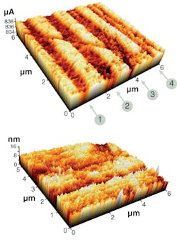
Bellouard and his collaborators are using a scanning thermal microscope (SThM; an atomic-force microscope equipped with a cantilever incorporating an embedded thermal probe) to detect femtosecond-generated index changes in fused silica. During scanning, the SThM cantilever follows the sample’s surface topology. From the resulting data, a topographic profile of the scanned surface is created. At the same time, the thermal probe locally heats the sample surface to a set temperature; the power needed to reach this target temperature is monitored, and from this data a thermal map is obtained. The two data sets are compared to identify local changes of thermal conductivity resulting from material changes.
With a Ti:sapphire laser producing 100 fs pulses at 800 nm and a 250 kHz repetition rate, the researchers wrote parallel lines at varying spacings in a 15-mm-wide sample of high-purity fused silica (Dynasil 1100), all of them 400 µm below the surface. The lines were written at a rate of 500 µm/s in the same scanning direction. The finished sample was cut with a diamond saw, then polished for examination with the SThM; topography and thermal-conductivity properties were measured (changes in thermal conductivity and in refractive index are both caused by the femtosecond pulses, and are thus intimately related).
Higher refractive index does not necessarily mean densification in the traditional sense (that is, more matter), notes Philippe Bado, one of the researchers. Although fused silica is amorphous from a global point of view, on a short scale it exhibits some order in the form of rings of molecules; when exposed to femtosecond pulses, the proportion of smaller rings increases.3 “We believe this results in a change in refractive index (the molecular bonds in the small rings are more ‘stressed’) without requiring more material,” says Bado.
The SThM allowed the researchers to detect the thermal footprint associated with femtosecond-generated waveguides. The associated refractive-index change was measured to a spatial accuracy of better than 50 nm. With this precision, manufacturing defects associated with the direct-write process and related hardware were clearly visible (see figure). Bellouard and his colleagues are now using this data to improve the waveguide-manufacturing process.
“To date, writing waveguides in fused silica with femtosecond pulses is a rather slow process,” says Bado. “The processing speed depends on numerous factors (including the desired optical quality of the waveguide, index difference between the core and the cladding, cross-section shape, and ability to carry long wavelengths such as 1550 nm). It is typically in the 20 to 500 µm/s range. Using the thermal data collected by Professor Bellouard, we intend to improve the efficiency of the writing process. For example, we are looking at improving the writing optics (spot size, spot symmetry, and so on) using the thermal data. Hopefully, this will result in a faster writing speed and will increase the commercial potential of this technique.”
REFERENCES
1. K.M. Davis et al., Optics Letters 21 (November 1996).
2. Y. Bellouard et al., Applied Physics Lett. 89, 161911 (2006).
3. J.W. Chan et al., Optics 26 (November 2001).

John Wallace | Senior Technical Editor (1998-2022)
John Wallace was with Laser Focus World for nearly 25 years, retiring in late June 2022. He obtained a bachelor's degree in mechanical engineering and physics at Rutgers University and a master's in optical engineering at the University of Rochester. Before becoming an editor, John worked as an engineer at RCA, Exxon, Eastman Kodak, and GCA Corporation.