PHOTODIODE ARRAYS: Amorphous-silicon approach beats the temperature challenge

Electronic devices on flexible substrates are a hot area of research, but there are as many problems associated with their manufacture as there are potential applications for them. But a team of researchers at the Palo Alto Research Center in California has made it a slightly less hot area of research, showing amorphous-silicon-based photodiode arrays at process temperatures much lower than the typical 210°C. Better yet, they use inkjet-printing of the etch masks for the backplane, a promising result for large-scale arrays on the cheap.1
Hydrogenated amorphous silicon (a-Si:H) sensors are known to have more defects when processed at lower temperature, and charge carriers can more easily recombine at defects. The result is low external quantum efficiency, or EQE (current out for photons in)-deadly for sensor applications. But the process temperature is the variable that causes the most headache in device design, because the diverse layers of flexible device structures suffer from mechanical stresses. Clearly, a lower temperature approach that maintains device integrity is needed.
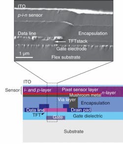
With that in mind, TseNga Ng and colleagues started with polyethylene naphthalate (PEN) and glass substrates. The a-Si:H p-i-n structures, coated with an unpassivated indium tin oxide layer, were prepared by plasma-enhanced chemical-vapor deposition (PECVD) at process temperatures from 130°C to 210°C. The lower process temperatures naturally reduced the efficiency of the devices, but by varying the thickness of the i layers, the team was able to optimize the temperature/thickness combination. Reducing the i-layer thickness brings about a concomitant reduction in absorption, but the interplay with the defects ensures an optimum thickness at a given temperature. For a 150°C processing temperature and 0.6-mm-thick i layer, the team found an EQE of 70%. While this number is somewhat lower than the best achievable in typical high-temperature processing, it is remarkably high at low temperature. The team found higher EQE on the PEN substrates than on glass.
Inkjet printing opens door to large arrays
With the device structure thus optimized, the team went on to integrate them with a thin-film-transistor (TFT) backplane to create a sensor array. The backplane was patterned using inkjet printing of the etch masks, with the TFTs and an encapsulation layer of oxynitride again made using PECVD. The approach stands in contrast to the laborious and expensive photolithography typical in sensor-array manufacture. The result is a 180 × 180 array, at 75 detectors per inch, and a sensitivity of 1.2 pW/cm2. The prototype device can operate at up to 20 Hz, with 14-bit dynamic range.
The digital-lithography part of the process is probably the most promising aspect of the work. “This type of digital lithography has attracted a lot of attention from academia and industry for reducing manufacturing cost for conventional electronics, displays, and sensor applications,” says Yongtaek Hong of the Advanced Flexible Device and Electronics Laboratory at Seoul National University.
TseNga Ng, the lead author of the studies, agrees. “The development of the a-Si:H sensor materials at low temperature enables fabrication of flexible sensor arrays within the temperature constraints of plastic substrates, minimizes film cracking, and will lead to low-cost roll-to-roll processing of large-area electronics,” says Ng.
Besides making it cheap, the digital-lithography approach makes minute control of the manufacturing possible. “The digital lithographic process also allows easy adjustment to local and global distortions in the flexible substrate during patterning, unlike conventional patterning techniques,” says Ng.
However, device operational stability is key for the low-temperature versions of devices. While the prototype looks like a clear winner for maximum manufacturing flexibility, Hong warns that commercial applications will have to wait until the devices have been put to longer-term tests.
While the research came out of a collaboration with Varian Medical Systems (Palo Alto, CA), the likely first application the team will pursue is border control. “The next step in this research is to develop large-area image sensors for cargo scanning,” Ng says, “with the goal of reducing the cost of large-area scanners that will go into ports of entry in the U.S.”
The group is interested in extending the approach using its expertise with organic semiconductors, to make even more cost cuts in large-area sensor-array applications. The inkjet process can then combine the patterning and deposition of metals, dielectrics, or semiconductors all in one step. While organics are known to result in low device EQE, and to date have low stability, the current optimization work makes for a brighter outlook for the organic semiconductor version. As Hong says, the team continues to be “the leading group in the field.”
REFERENCES
1. TseNga Ng et al., Applied Phys. Lett.91, 063505 (2007).
D. Jason Palmer | Freelance writer
D. Jason Palmer is a freelance writer based in Florence, Italy.