The idea of integrated optics was born as a logical extension of integrated electronics. As the concept was originally described by Stewart Miller of Bell Labs in 1969, integrated optics were intended to combine discrete optical elements on a monolithic substrate that could be mass-produced like integrated-circuit chips.1 Over the years, the concept evolved into integrated photonics, including active elements such as lasers, modulators, and detectors. But although some integration has been demonstrated, the degree of miniaturization has been limited by the size of photons and the optical devices needed to manipulate them.
Now a new paradigm for integrating optical nanocircuits has been proposed by Nader Engheta, an electronic engineering professor at the University of Pennsylvania (Philadelphia, PA). Instead of starting from the concept of optical devices, he begins with circuit elements like those used in electronics-but shrunk to a nanoparticle scale-and takes advantage of the emerging field of optical metamaterials. Although these nanocircuit elements are much smaller than an optical or infrared wavelength, he points out that electronic-circuit elements used in radio-frequency and microwave circuits are miniscule compared to the frequencies they handle.2
The analogy between subwavelength devices at optical frequencies and radio frequencies is far from exact. A crucial difference is that, instead of simply inducing conventional flow of conduction-band electrons through metallic conductors, optical-frequency signals induce collective oscillations of conduction-band electrons on plasmon resonances at the surfaces of some noble metals. In suitable metals, such as silver, the real part of the electrical permittivity ε is negative at optical frequencies. Applying an optical field produces an electric displacement current density (∂D/∂t from Maxwell’s equations) that describes the subwavelength-scale “flowing optical current.”
Describing nano-optic circuit elements
The electrical impedance of conventional circuit components-capacitors, inductors, and resistors-describes their response to the electric fields applied by electronic signals. To derive the analogous optical impedance of a nanoparticle, Engheta’s group calculated the flux of optical-electric displacement current into and out of the nanoparticle, and the optical-electric potential averaged over the nanoparticle. The ratio of the two quantities is an optical impedance that corresponds to the electrical impedance of an electronic component.
The optical impedance depends on the particle composition, its size and shape, and the optical frequency. Composition is critical because it determines the optical-frequency permittivity ε. In conventional dielectrics such as silica, the real part of the permittivity is positive so the nanoparticle acts as a nanoscale capacitor. In noble metals the real part of permittivity is negative, so the nanoparticle behaves as a nanoscale inductor. An imaginary part of the permittivity represents loss at optical frequencies, corresponding to electrical resistance; loss is particularly low in silver, so it is preferred for plasmon generation. This approach allows the use of tools developed for analyzing the response of electronic RLC (resistive-inductive-capacitive) networks that are taught in standard courses on electronic network theory. Just as virtually all real electronic components have some electronic resistance, virtually all optical materials have some optical loss.
Electronic circuits require two additional classes of devices-conductors with near-zero impedance to transmit electronic currents between components, and insulators with near-infinite resistance to block leakage between conductors. These have counterparts in Engheta’s model. “Epsilon very large” (EVL) materials have very high permittivity, so a small optical-frequency field produces a large displacement current, the equivalent of conductors. “Epsilon near zero” (ENZ) materials produce very small displacement currents, the equivalent of insulators.
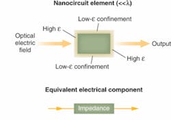
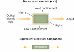
Permittivity is a function of frequency. Natural materials dont always exist with the desired value of permittivity at a particular optical frequency, but optical metamaterials can be designed to have the desired value. For example, subwavelength layers of a plasmon-supporting metal such as silver can be stacked with alternating subwavelength layers of a conventional dielectric. Depending on the materials and layer thicknesses and the orientation of the electric field, the resulting optical metamaterials will have either near-zero or very large permittivity. Covering optical nanoparticles with layers of these materials can control their behavior. Layers of EVL materials, for example, could be coated on the two ends of a nanoparticle, with displacement-current-blocking layers of ENZ materials on the sides. An ambient optical field then would affect the front, and a processed version would emerge from the other end (see Fig. 1).
Assembling ‘metananocircuits’
Engheta envisions a “metananocircuit” containing many individual subwavelength optical nanoelements built of different materials, just as integrated circuits contain many individual electronic components. The optical metananocircuit would modify optical signals, just as an electronic circuit modifies electronic signals. Naturally the details differ.
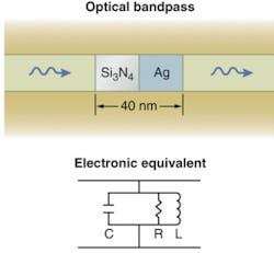
One simple example is a bandpass filter. Electronic bandpass and bandstop filters contain a capacitor, inductor, and resistor in parallel or in series. Two optical nanoelements could form a similar metananocircuit, says Engheta. One is a nanoscale inductor made from a plasmonic metal such as silver, with its internal loss providing the resistive part of the circuit. The other is a nanocapacitor formed from a conventional dielectric material. Placing the two nanoelements between a pair of parallel plates that define an impenetrable waveguide would form an optical bandpass filter (see Fig. 2). Engheta has validated the optical circuit in a computer model, and is planning an experimental device.
Adding more nanomodules would allow metananocircuits to perform other functions. Stacking together multiple nanocapacitors and nanoinductors could produce the optical counterparts of electronic circuits with the components arranged similarly. Engheta’s computer model shows that the distribution of electric fields from a metananocircuit assembled from three nanoinductors and three nanocapacitors resembles the behavior of a similar electronic circuit.
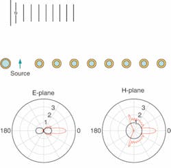
Another case Engheta has modeled is an optical counterpart of the Yagi-Uda antenna used at radio frequencies. The electronic version aligns several parallel conducting wires parallel to a radiating dipole antenna-one long wire is left of the radiating dipole, and several shorter wires are on the right (see Fig. 3). This arrangement of wires directs the dipole radiation toward the right of the figure, suppressing the natural dipole field. The nano-optical version replaces the parallel wires with silver nanospheres covered with dielectric shells, and the radio-frequency dipole with an optical dipole emitter such as a quantum dot. Like the radio-frequency version, the single element of the optical antenna (left) differs in size from the many identical elements (right). The calculated radiation pattern for the optical antenna is compared with the dipole field in two different planes in the lower part of the figure.3
Engheta says the optical antenna design could be taken further, by arranging two or more arrays resonant at different optical frequencies around a single emitter. Then each antenna would generate a beam at its resonant wavelength pointed in a different direction.
Outlook
The field of metananocircuits is new enough that it is still in search of a name. In a review paper in Science (Sept. 21, 2007), Engheta called the field “metactronics” as shorthand for “metamaterial-inspired nanoelectronics.” So far, devices exist only on paper and in computer models, although Engheta is talking with experimentalists about building proof-of-concept devices. But the new paradigm holds out exciting possibilities of a whole new class of devices and integration.
On one level, the circuit paradigm could serve as a building block for new types of metamaterials, for use in optical nanocircuits or for other applications. The circuit paradigm also could lead to new types of devices, such as switches and new ways to divide signals. Other possibilities include bringing nonlinearity down to the optical nanocircuit scale for applications such as modulation or active devices.
The optical nanocircuit approach also might be extended to developing an imaging system with far-field resolution of less than half a wavelength, a distance below the diffraction limit.4 Engheta reports that others have arrived at a similar idea for far-field subwavelength imaging, using another method, and demonstrated it using different approaches.5, 6, 7 He doesn’t know how it’s going to turn out, but the fresh approach could break old bottlenecks.
REFERENCES
1. S.E. Miller, The Bell System Tech. J. 48(7) 2059 (1969).
2. N. Engheta, Science 317, 1698 (Sept. 21, 2007)
3. J. Li, A. Salandrino, and N. Engheta, www.arxiv.org/abs/cond-mat/0703086 (2007)
4. A. Salandrino and N. Engheta, Physical Rev. B74, 075103 (2006)
5. Z. Jacob, L. V. Alekseyev, E. Narimanov, Opt. Express 14, 8247 (2006).
6. Z. Liu, H. Lee, Y. Xiong, C. Sun, X. Zhang, Science 315, 1686 (2007).
7. I. I. Smolyaninov, Y. J. Hung, C. C. Davis, Science 315, 1699 (2007).
Tell us what you think about this article. Send an e-mail to [email protected].


