Technology Review 2007: Photonic solutions find no lack of real-world problems
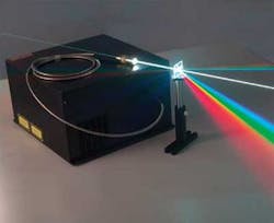
The first working laser, almost 50 years ago, was described jokingly as a solution looking for a problem. Attempts by significant portions of the laser industry to redefine it as a “telecom” industry less than a decade ago, indicates that the old joke, to some degree, may still apply. The emergence of broadly applicable fiber-laser technology, however-enabled largely by telecom-era R&D-as both a competitor for conventional laser applications and as a means of extending laser technology to new application areas presents an intriguing challenge (see Fig. 1).
Rather than redefine the market served, fiber lasers appear to redefine “laser technology” in ways that de-emphasize optical approaches that have traditionally constituted the bedrock of laser development and design. While other emerging optical developments-organic emitters, quantum dots, and silicon photonics-might also be thought of as redefining the technology, fiber lasers appear to do it for established laser applications, thereby posing a significant challenge to an established industry heavily invested in applying traditional methods to traditional applications.
Regardless of the ultimate outcome of the current rapid expansion of fiber-laser technology, the fact that most of the major players in the conventional laser industry announced fiber-laser programs and products this year is likely to be remembered as a big deal. Will it be as big a deal for the laser industry as the transition from fossil to renewable sources for the energy industry? No, not for fiber lasers alone: but the combined effects of emerging and improving source and detector technologies in 2007-which also include quantum dots, silicon photonics, organic photonic devices and solid-state UV sources-indicate that the laser industry will probably look quite different at the end of the 21st century than it did at the end of the 20th. Joking aside, based on the state of the art in 2007, laser technology could be quite accurately characterized today as a solution for many problems.
Fiber here, fiber there
In January, Newport (Irvine, CA) announced formation of a new Fiber Laser Business Group within its Spectra-Physics Lasers Division. And four months later, it introduced a diode-pumped solid-state laser that uses a master-oscillator power fiber-amplifier (MOPFA) design with a modelocked seed laser to deliver 12 W in 355 nm picosecond pulses at an 80 MHz repetition rate. The device is targeted at OEM processes such as precision cutting, dicing, scribing, and ablation for new and existing applications in the microelectronics and industrial manufacturing markets, including semiconductors, solar cells, automobiles, and flat-panel displays.
Also in January, fiber-laser manufacturer IPG Photonics (Oxford, MA), after completing its first full year as a public company with 23% annual revenue growth, introduced an industrial scanning system for high-speed spot welding and drilling that combines fiber-laser technology with processing technology developed by Reliant Technologies (Mountain View, CA) for use in medical devices. The resulting industrial scanner provides rapid dwell times at preprogrammed locations at frequencies up to 5 kHz, and can be programmed to apply medical levels of thermal management to manufacturing processes in computer, consumer electronics, and aerospace industries.
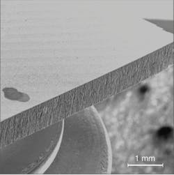
In addition, fiber-laser manufacturer SPI Lasers (Southampton, England), which entered 2007 reporting 100% year-on-year growth in sales for 2006, announced its entry into a new application area, diamond processing (see Fig. 2).Fiber Laser 2007
Laser 2007 in Munich in June was particularly marked by the introduction of new fiber lasers as well as fiber-laser firsts from traditional laser manufacturers (see wwww.laserfocusworld.com/articles/302470). Newport demonstrated a new high-power fiber-laser platform consisting initially of single-mode 100 and 200 W continuous-wave fiber lasers for high-precision industrial applications, such as laser cutting of metal and nonmetal materials, laser spot and seam welding of thin metal, and bonding and welding of plastics. Other potential applications include reprographics and printing applications, selective metal sintering for functional prototypes or small production runs, as well as for tool and die molds and photovoltaic manufacturing applications such as solar-cell singulation, isolation, scribing, and structuring.
“We believe that this new fiber-laser platform represents a paradigm shift for many industrial applications that have previously been served by conventional lamp-pumped and diode-pumped solid-state (DPSS) technologies because it offers inherent advantages in cost and performance efficiency, power scalability, reliability, and beam quality for many applications,” said Wolfgang Gries, senior director of Newport’s Fiber Laser Business Group.
Announcements by SPI Lasers included a U.S. patent for the company’s GTWave composite fiber technology, in which the active and pump fiber, surrounded by a common coating enables gradual diffusion of pump fiber into active fiber to prevent hot spots during pumping at high power. SPI Lasers also launched the next generation of its MOPA-based pulsed-laser technology in Munich, including new features such as a fully integrated single-unit laser controller, direct pulse triggering that allows on-the-fly variations, an enhanced package of 25 preset waveforms, faster analogue control that enables grayscale and bit-map applications, hardware control for faster communications, and an improved beam-delivery optic with fully integrated isolator (see www.laserfocusworld.com/articles/302492). In addition, SPI announced two new OEM laser modules for integration into kilowatt- and multikilowatt-power cutting and welding solutions, a 400 W stackable laser module and a 400 W laser resonator.
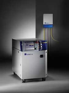
Trumpf (Ditzingen, Germany) entered the fiber-laser market in Munich with a single-mode fiber laser producing 300 W of power, at a beam quality, M2, of better than 1.1, for precision cutting and welding of items such as batteries, hard-disk mountings, pacemakers, sensors, electromechanical components, thin sheets, foils, scanners and cell-phone casings (see Fig. 3). GSI Group Laser Division (Rugby, England) launched a new range of rack-mountable ytterbium industrial fiber lasers with power levels up to 4 kW.IPG introduced a commercial 3 kW continuous-wave ytterbium single-mode fiber laser in Munich. The laser was billed as the “first low-cost alternative to e-beam technology” for applications such as deep-penetration welding, remote welding and cutting, percussion drilling, and fuel-cell welding. IPG also expanded its ytterbium pulsed-fiber-laser product line, targeted at marking and new materials processing applications in the manufacturing of silicon wafers, plasma, and LCD display screens, and other devices. The new IPG introductions more than doubled maximum power output levels in more than one product line.
“With the expanded pulsed-laser line, IPG’s fiber lasers provide an alternative to conventional lamp-pumped and diode-pumped crystal pulsed lasers in a range of applications requiring higher powers because of the proven cost, efficiency, beam quality, and reliability of fiber lasers,” said Valentin P. Gapontsev, IPG CEO. IPG is also developing higher-power models for introduction in the future and expects to release additional pulsed-laser lines, including a 150-kW-peak-power laser, a 1 to 20 ns tunable laser for high-contrast marking, and a laser family offering direct triggering of 50 ps pulses with peak power up to 250 kW.
The fiber pace did not lessen after Munich, either. In August, IPG announced a $3.8 million contract with the U.S. Naval Warfare Surface Center to supply a 44 kW fiber-laser system, consisting of eight commercial 5.5 kW fiber lasers. In September, SPI Lasers announced promising results in processing 0.2- to 0.8-mm-thick polycrystalline silicon used in solar-cell production using a 200 W 1070 nm CW fiber laser. It also announced an extension to its pulsed-laser product range for marking applications.
In October, previous Rofin-Sinar (Hamburg, Germany) acquisitions-80% of high-power laser-diode maker m2k-laser (Freiburg, Germany), fiber-laser manufacturer Corelase Oy (Tampere, Finland), and laser-marking systems provider ES Technology (Oxfordshire, England)-yielded fiber lasers at 100 W and 200 W power levels, based on technology from SPI Lasers, for cutting and welding applications.
Solid-state UV sources
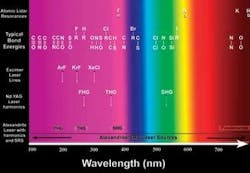
Fiber lasers generally emit in the ytterbium wavelength range around 1064. The fact that Newport’s first fiber-laser product was a UV source is an indication of the versatility of fiber-laser technology, as well as another area of important technology development in 2007 aimed at a particular section of the UV spectrum. Between the mid-power deep-ultraviolet (DUV) applications served by excimer lasers and the low-power, near-UV information-storage and biomedical applications served by diode lasers, lies more than 99% of the UV spectrum and a vast range of applications associated with atomic and molecular electronic structure, which increasingly demand versatile, user friendly, and relatively inexpensive UV sources (see Fig. 4). The ongoing evolution of tunable and fixed-wavelength UV sources based on alexandrite laser technology is helping to address many of these applications ranging across basic physics, remote sensing, molecular detection, combustion research, and optical metrology (see www.laserfocusworld.com/articles/294651).In October, alexandrite laser technology patented by Laser Energetics (Princeton, NJ)-which incorporates an Nd:YAG laser pump as its excitation source to create tunable light in IR, UV, or DUV wavelengths-advanced to the proof-of-concept stage in a U.S. Army selection process for a near-term “remote sensing” application for detecting chemical-warfare agents. Coherent (Santa Clara, CA) introduced an 8 W 355 nm solid-state, quasi-CW Paladin laser for the peacetime pursuit of laser direct imaging (LDI) of high-density printed-circuit boards, as well as semiconductor wafer inspection, with potential for other markets, including semiconductor processing or glass scribing.
Crystal IS (Green Island, NY) was awarded a three-year $2 million contract from the National Institute of Science and Technology (NIST; Gaithersburg, MD) Advanced Technology Program to investigate the performance of low-defect aluminum nitride substrates in various crystal configurations, with the ultimate goal of developing 280 nm light-emitting diodes that will operate at high powers and high efficiencies over long lifetimes. The field of UV processing and analytics has opened up many applications over the past several years in areas as wide-ranging as homeland security, water and air disinfection, and in the UV curing of inks and polymers. Market growth remains technology limited in many applications, however, where a small, durable, mercury-free light source might be better suited.
In the area of solid-state lighting, LedEngin (Santa Clara, CA), a supplier of high-power LED components and light-source modules, began shipping customer samples in the first quarter of 2007 and now has several products shipping in volume, including new UV and multiwavelength UV LEDs for medical, portable, and other applications. “We are excited to enable a host of applications requiring ultra-high-power UV-based LED lighting,” said David Tahmassebi, president and CEO, noting that traditional UV lamps are bulky, expensive, and have a short lifespan that requires UV bulbs to be replaced often.
The commercial availability of UV LEDs in the near-UV 365 to 400 nm range is enabling the development of digital UV imaging, in which a commercial UV camcorder, such as the UVCorder introduced by Oculus Photonics (Goleta, CA), provides imagery for a range of applications in fields such as forensics, laser technology, biology, art conservation, and defense. The UVCorder is based on a CCD-array camera optimized for reflected UV imaging and is packaged for the R&D and industrial inspection markets. The system comes with an adjustable-aperture lens and a near-UV LED light source.
Organic photonics
Organic photonic materials continue to evolve toward the ultimate promise of significant advantages in terms of flexibility, power consumption, and cost over traditional semiconductors for a wide range of applications. The current niche is primarily in small displays, but improving lifetime, efficiency, and cost should help them spread widely in handheld devices (see www.laserfocusworld.com/articles/282671). Excitement in the field remains high, however, maintained in large part by constant new developments, such as Sony’s plan to commercially launch an organic-LED (OLED) television in the Japanese market this month. The screen size will only span an 11 in. diagonal, but in addition to the high contrast, high peak brightness, good color reproduction, and rapid response time that Sony promises, the very low power requirements of OLED technology could eventually enable a significant step toward replacing wall plugs with power over Ethernet, so far largely limited to telephones, wireless access points, and security cameras.1, 2
A phosphorescent dye molecule that emits near-IR light is under investigation at the University of Southern California for making long-lasting organic light-emitting diodes (OLEDs) that might be used to make a cheap and flexible near-IR display, unreadable to the naked eye but visible through night-vision goggles. Such OLEDs might also be converted into night-vision enabling diodes by depositing the thin organic polymers on substrates, including the bendable plastic of a helmet visor. A phosphorescent dye molecule in the emissive layer sandwiched between the device’s two electrodes emits very efficiently in the near-IR region. The device itself emits right at the border of the visible and near-IR spectrum, close to 800 nm at an efficiency in excess of 6%.3
The potential for organic photonic materials to produce thin-film photovoltaics (TFPV) at relatively low cost and weight on flexible substrates-and to embed solar-power capabilities into walls, roofs, and even windows-is driving TPFV manufacturers to ramp up production capacity, and several companies are building plants with more than 100 MW capacity (see www.laserfocusworld.com/articles/302958).
Quantum dots
Emerging silicon nanocrystal or “quantum-dot” technology also holds significant promise for impacting photovoltaics, as well as several other areas. Researchers at the U.S. Department of Energy’s National Renewable Energy Laboratory (NREL; Golden, CO), collaborating with Innovalight (Santa Clara, CA), have observed a significant capacity for multiple exciton generation (MEG)-formation of more than one electron per absorbed photon-in silicon nanocrystals. As a result of this collaboration, silicon nanocrystals obtained from Innovalight can produce more than one electron from single photons of sunlight that have wavelengths less than 420 nm, essentially providing a potential avenue for converting a portion of the solar energy lost as heat (50%) into electricity (see www.laserfocusworld.com/articles/301818).
At the Rice University (Houston, TX) Center for Biological and Environmental Nanotechnology researchers described a 90% efficient recipe that also appears to offer “greener” chemistry and scalability for fabrication of photovoltaic and electronic devices using cadmium selenide (CdSe) quantum dots with a four-legged, or tetrapod, structure. Upon incorporating quartenary ammonium salt (QUAT) compounds such as cetyl-trimethyl-ammonium bromide or didodecyl-dimethyl-ammonium bromide into the hot-injection-synthesis process, the research team observed a more than 100% increase from typical 40% efficiencies to 90% for producing CdSe tetrapods. The researchers described their work as a key step toward quantum-dot-based photovoltaics as an alternative to more-expensive silicon-based solar cells (see www.laserfocusworld.com/articles/294623).
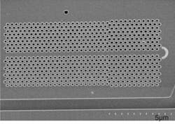
Despite the hopes of early developers, quantum dots have generally not worked well as lasers, yet efforts to improve performance continue. A team from the University of Tokyo reported room-temperature CW lasing at 1.3 µm from a photonic-crystal nanocavity using a quantum-dot active layer. Despite stable optical output when the optical pump power was just above threshold, they found that long-term pumping at 1.5 times the threshold could damage the cavity (see Fig. 5; www.laserfocusworld.com/articles/294657). Researchers at the University of Southern California (Los Angeles, CA), the University of Texas at Austin (Austin, TX), and the University of Central Florida (Orlando, FL), however, have demonstrated an edge-emitting photonic-crystal (PC) nanocavity laser (see Fig. 4). Pumped from the top by an 850 nm laser diode, the PC laser emits at approximately 1330 nm (see www.laserfocusworld.com/articles/294627).Silicon photonics
Silicon photonics continue to approach III-V performance levels and commercial availability. A CMOS-compatible 10 Gbit/s optoelectronic transceiver is under development at Luxtera (Carlsbad, CA). Silicon’s 1.1 µm band edge requires the use of longer wavelengths (typically 1.5 µm) to transmit light through a silicon waveguide, and at the same time rules out the use of silicon as a photodetector material. So germanium (Ge) is the usual replacement, in the form of a hybrid photodetector. In collaboration with Freescale Semiconductor (Austin, TX), Luxtera has used CMOS processing to seamlessly integrate a 1.5 µm detector with its receiver electronics. At 10 Gbit/s and an average detector power of -14.2 dBm, the complete receiver has a bit-error rate of 10-12 (see www.laserfocusworld.com/articles/292384).At Intel, research has been focused on modulators, hybrid lasers, and photodetectors as building blocks for silicon photonics (see www.laserfocusworld.com/articles/292401). And this year, researchers at Intel reported a germanium-on-silicon photodetector capable of operation at 40 Gbit/s to complement previously demonstrated silicon-based lasers and modulators. The next step, according to the company is to combine all three devices on a single silicon chip (see Fig. 6).
REFERENCES
1. www.ledsmagazine.com/news/4/10/6
2. www.accountancyage.com/business-green/news/2201123/organic-leds-revolutionise
3. www.technologyreview.com/Infotech/18120/?a=f
Hassaun A. Jones-Bey | Senior Editor and Freelance Writer
Hassaun A. Jones-Bey was a senior editor and then freelance writer for Laser Focus World.
