QUANTUM-CASCADE LASERS: Harvard engineers pioneer plasmonic QC laser nanoantennas
In a move that may open up a whole new area of optoelectronics, Harvard University (Cambridge, MA) engineers have demonstrated a plasmonic quantum-cascade laser nanoantenna capable of providing nanometric-scale chemical imaging of a wide range of materials and biological specimens in unprecedented detail. The antenna is used to concentrate light to the subwavelength scale.
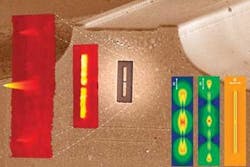
Graduate students Nanfang Yu and Ertugrul Cubukcu worked with Federico Capasso, the Robert L. Wallace professor of Applied Physics at Harvard’s School of Engineering and Applied Sciences, to target the “molecular fingerprint region” of the spectrum. They designed a device with two gold rods separated by a nanometer gap—an optical antenna—built onto the facet of a quantum-cascade (QC) laser that emits at 7 µm into the region of the spectrum where most molecules have absorption fingerprints (see figure).
“We essentially take a laser and apply a thin, insulating layer of 100-nm-thick aluminum oxide to the facet of the laser, because if you put metal directly on the facet of the laser it would electrically short it,” Capasso says. “Next, we apply a thin layer of gold. Then, using a focused ion beam, we sculpt the antenna by taking away the gold and defining it through metallic routes.”
The length of the antenna must be along the direction of polarization of the laser, says Capasso, because the electric field of the laser radiation makes the electrons of the metal oscillate when it’s directed along the rods. “The length of each arm of the antenna is basically equal to half a wavelength,” he explains. “It’s a resonant antenna that provides a very strong charge oscillation and creates a very strong electric field right where the actual gap is. This near field comes from the surface plasmons, which are the oscillations of electrons within the metal, and you can achieve a large enhancement of the electric field inside the gap to generate very intense laser nanospots of a size about 100 times smaller than the laser wavelength right at or near the surface of the laser. Then the spot can be scanned across a specimen to provide superior spatial resolution.”
High-density optical storage
Capasso and colleagues reported a similar laser nanoantenna concept last year at a very different wavelength for a different application (see www.laserfocusworld.com/articles/274712). “That device was designed for 8,000 Å, which is a ten times smaller wavelength,” says Capasso. “We could get smaller spots there, and we’ve been talking to industry about it for optical storage-extremely high density DVDs.”
Quantum-cascade lasers were invented and first demonstrated by Capasso and his group at Bell Labs in 1994. The millimeter-length semiconductor lasers, which are now commercially available, are made by stacking nanometer-thick layers of semiconductor materials on top of each other. By varying the thickness of the layers, one can select the wavelength of the QC laser across the entire infrared spectrum where molecules absorb-enabling custom design for a specific application. They’re also widely tunable and have a broad range of applications, including chemical sensing, pollution monitoring, and medical diagnostics.
What’s next? “Now we’re studying different types of antennas, such as ‘bowtie’ ones, where you can get more intense and concentrated spots in the gap and reduce the intensity of the spots at the edges of the antenna at the opposite extremes because there’s less charge accumulation,” Capasso says. “This allows you to cut down on stray light and so forth.”
In the future, there’s little doubt that optical storage will need to move to subwavelength techniques to continue on the curve of increased density. “We’re receiving lots of interest in partnering with companies to do research on optical storage applications with the antenna technology,” notes Capasso.
The researchers have filed for U.S. patents covering this newest class of photonic devices, but it may take five to ten years before products using QC laser nanoantenna technology become commercially available-based on the typical timeframe of R&D demonstration to product launch.

Sally Cole Johnson | Editor in Chief
Sally Cole Johnson, Laser Focus World’s editor in chief, is a science and technology journalist who specializes in physics and semiconductors. She wrote for the American Institute of Physics for more than 15 years, complexity for the Santa Fe Institute, and theoretical physics and neuroscience for the Kavli Foundation.
