Evanescent polarization-induced technique enables nanometer-scale imaging

March 1, 2007
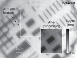
Using a solid-immersion lens (SIL), which does not affect or contaminate the sample like liquid-immersion systems and also enables imaging at numerical-aperture (NA) values greater than 2, researchers in the College of Optical Sciences at theUniversity of Arizona (Tucson, AZ) have demonstrated an induced-polarization evanescent-imaging technique that achieves nanometer-scale vertical resolution and high lateral resolution over a relatively large field of view.

Using a solid-immersion lens (SIL), which does not affect or contaminate the sample like liquid-immersion systems and also enables imaging at numerical-aperture (NA) values greater than 2, researchers in the College of Optical Sciences at theUniversity of Arizona (Tucson, AZ) have demonstrated an induced-polarization evanescent-imaging technique that achieves nanometer-scale vertical resolution and high lateral resolution over a relatively large field of view.

Click here to enlarge image

The flat side of the hemispherical SIL is placed just above the sample to be measured. The small gap height (less than the wavelength of the imaging light) enables contrast-enhanced evanescent coupling of the light between the SIL and the sample, inducing a polarization state at the pupil of the objective lens. This information is then imaged onto a CCD and analyzed using a vector plane-wave decomposition model to determine the physical dimensions of the sample under test. Experiments using a patterned silicon wafer and a known reference target with NA of 1.5 confirm a lateral resolution of approximately 175 nm (better than a conventional far-field microscope without scanning or immersion oil) and a height accuracy of ±2 nm in a 25 µm field of view. Contact Tom Milster at [email protected].
Sponsored Recommendations

Brain Computer Interface (BCI) electrode manufacturing

Jan. 31, 2025
Learn how an industry-leading Brain Computer Interface Electrode (BCI) manufacturer used precision laser micromachining to produce high-density neural microelectrode arrays.

Electro-Optic Sensor and System Performance Verification with Motion Systems

Jan. 31, 2025
To learn how to use motion control equipment for electro-optic sensor testing, click here to read our whitepaper!

How nanopositioning helped achieve fusion ignition

Jan. 31, 2025
In December 2022, the Lawrence Livermore National Laboratory's National Ignition Facility (NIF) achieved fusion ignition. Learn how Aerotech nanopositioning contributed to this...

Nanometer Scale Industrial Automation for Optical Device Manufacturing

Jan. 31, 2025
In optical device manufacturing, choosing automation technologies at the R&D level that are also suitable for production environments is critical to bringing new devices to market...

Voice your opinion!

To join the conversation, and become an exclusive member of Laser Focus World, create an account today!