Long-wave infrared detectors: Inspired by nature, IR detector targets long-wavelength applications
OMER GOKALP MEMIS AND HOOMAN MOHSENI
The infrared spectrum has always offered possibilities beyond human visual capabilities. Infrared (IR) detectors have found their place in many applications, and have been indispensable tools for looking at objects from a different perspective to investigate less-evident properties. As a result, there has been ongoing research in IR-detector technologies, exploring different approaches with a wide range of material systems.1 These steady advances in technology constantly require better and more sensitive detectors for demanding applications, which has led to the need for the ultimate photon sensors: single-photon detectors.
Single-photon detectors (SPDs) are ultra-low-noise devices with increased sensitivity to be able to detect a minimum energy quantum of light-the photon. These SPDs can sense and count individual photons and can be utilized in many emerging applications in which the only available signal is on the order of several photons. Using a bioinspired approach based on the light-detection mechanism in the rod cells of the eye, our research groups at Northwestern University and the University of Illinois have developed an IR single-photon focalized carrier augmented sensor (FOCUS). The possible applications for FOCUS include biophotonics, medical tomography, nondestructive materials inspection, homeland security and surveillance, military vision and guidance, and quantum imaging and cryptography.
Challenges for IR detection
The biggest challenge for IR detectors is realization of a device that can create an adequate signal-to-noise ratio. To achieve this, the detector should efficiently absorb light at a particular wavelength, it should have noise lower than the signal, and it should be coupled with read-out electronics that have similar low-noise properties. For IR SPDs, these constraints are particularly challenging because the optical signal power of a single photon is less than approximately 1 attoJoule. Increasing the wavelength further into long-wave IR (LWIR) and far-IR (FIR) spectra makes the photon extremely low energy, and introduces more problems.
In parallel, efficient absorption in any wavelength requires that the width of the absorbing layer (perpendicular to the propagation direction) be comparable to that particular wavelength. Therefore, in the LWIR and FIR region, the device dimension must be on the order of several microns to tens of microns. Unfortunately, reducing the electrical noise below the photon energy requires nanometer-size devices. The low energy of individual photons and large wavelength make the fabrication of low-noise and high-efficiency LWIR single-photon detectors inherently problematic.
Bioinspirations and operating principles
The ongoing research for single-photon IR detectors has led to specialized p‑i‑n detectors, avalanche photodetectors (APDs), single-electron-transistor-based detectors, and superconducting (transition-edge) detectors. Among the list, the main candidates for solid-state single-photon detectors without cryogenic cooling are APDs. However, IR-compatible APDs suffer from many problems, including increased noise due to the statistical nature of the avalanche gain, randomly triggered afterpulses, and increased dark current due to tunneling at the required high electric fields.2 Hence, their operation is limited to a few synchronized systems with special quenching circuits that allow above-breakdown voltages for extremely short durations.
To overcome the problems with solid-state single-photon detectors, our research groups study existing single-photon detectors in nature. The human visual system possesses the ability to detect single photons because of a particular type of light-sensitive cells, the rod cells.3 The rod cells owe their adaptation from dim-light gray-scale vision to their richness in a special molecule called rhodopsin.4 The geometry of a rod cell and the arrangement of rhodopsin in the cell provide large absorption volumes for efficient capture of photons. Furthermore, rhodopsin molecules, together with a series of other catalysts and messenger molecules, play an important role in the amplification of the detected signal before it gets contaminated with the noise of the processing neural systems. We tried to replicate these principles of the human visual system for efficient single-photon detection.
Developing FOCUS
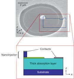
Although nanoscale features provide interesting properties such as ultralow capacitance and quantum effects, they suffer from low fill factor that prevents them from absorbing light efficiently. The FOCUS sensor utilizes large absorptive volumes in addition to nanoscale sensory features, allowing it to perform in a similar manner to the geometry of rod cells (see Fig. 1).
The operation principle of FOCUS is a replication of this biological mechanism in the electronic domain: when properly biased, electrons in the nanoinjector region of FOCUS want to move toward the large absorptive region because of the internal electric field. However, the end of the nanoinjector forms a barrier against this flow, blocking most of the electrons. When a photon strikes the large, thick absorption region it creates an electron-hole pair with high probability, and the hole is immediately attracted toward the nanoinjector with the aid of the built-in electric field. When the optically excited hole reaches the nanoinjector, it lowers the barrier. The ultralow capacitance of the nanobarrier makes it extremely sensitive to any change in total charge, lowering the voltage significantly with even a single additional hole. The lowered barrier lets more electrons into the absorption region, and the number of injected electrons increases exponentially with the amount of potential change. Thus, a single captured photon changes the injection current significantly because of the internal gain mechanisms and appropriate band structure.
Fabrication and results
After the layer structure and geometry of the devices were designed with a three-dimensional nonlinear finite-element-method (FEM) simulation, the epitaxial layers were grown using metal-organic chemical-vapor deposition. The wafers were patterned using e-beam lithography to form nanoscale features. An e-beam evaporator was used to deposit metal on these features, which double as a hard mask for the proceeding etching step: the features were etched first by reactive-ion etching and then by wet etching, finally forming the nanoinjectors. The void around the nanoinjectors was filled with passivation and planarization agents (polyimide or oxides) to improve surface quality and structural integrity. The final metallization step created the contact pads required for electronic integration.
The circular devices with diameters ranging from 100 nm to 5 µm were fabricated and tested. The primary target spectrum of these devices was the near-IR region. In a custom-prepared and calibrated setup, dark current, photocurrent, optical gain, spatial sensitivity, bandwidth, transient response and excess noise characteristics were measured. Devices under test were biased with voltages lower than 2 V.
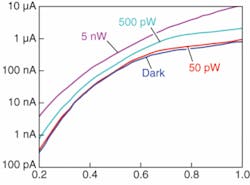
Calibrated continuous-wave lasers were used in dark and photocurrent tests. The measurements showed a significant increase in optical response while maintaining dark current values comparable to state-of-the-art APD detectors (see Fig. 2). Stable gain values exceeding 4000 were measured from small devices at low bias voltages, which suggest orders of magnitude increase over existing SPD alternatives. Also, the necessary bias voltage for FOCUS detectors is much lower than the required voltages for APDs, which can be as high as 50 V. The spatial sensitivity of the devices was measured using an automated setup, which confirmed our simulation predictions about the devices collecting carriers 6 to 7 µm away from the nanoinjectors.
The bandwidth of the FOCUS detectors was evaluated at different processing steps and a clear dependence of bandwidth on the surface quality has been observed, which is consistent with the expectation from a nanoscale device with very high surface-to-volume ratio. Unpassivated devices showed bandwidths reaching 400 kHz, whereas some specifically passivated ones exceeded 300 MHz. However, the increase in bandwidth was always accompanied with a reduction in gain, indicating a constant gain-bandwidth product of more than 3 GHz. Compared to APDs, which have bandwidth problems due to deep traps with long lifetimes and related afterpulsing, FOCUS detectors do not exhibit such unwanted side effects.
There have also been differences among different forms of passivation, which allow optimization in the tradeoff between gain and bandwidth. Correlated to bandwidth results, we have also made transient response measurements using an ultrafast femtosecond pulsed laser and optical attenuators. With some averaging, we were able to distinguish electrical pulses corresponding to the effect of five photons.
These FOCUS devices were designed and simulated with a custom-written nonlinear FEM simulator for NIR spectra. We believe that FOCUS will be improved as we gain more insight into nanoscale effects, refine corresponding fabrication processes, and extend operation to LWIR and FIR wavelength regions.
ACKNOWLEDGMENTs
The authors would like to acknowledge the partial support from DARPA and NSF for this project.
REFERENCES
1. A. Rogalski, Progress in Quant. Electronics 27(2-3) 59 (2003).
2. A. Lacaita et al., Applied Optics 35(16) 2986 (1996).
3. F. Rieke and D.A. Baylor, Rev. of Modern Physics 70(3) 1027 (1998).
4. S. Hecht et al., J. Gen. Physiol. 25(6) 819 (1942).
OMER GOKALP MEMIS is a student and HOOMAN MOHSENI is assistant professor in the Department of Electrical Engineering and Computer Science at Northwestern University, 2145 Sheridan Rd., Evanston, IL 60208; e-mail: [email protected]; www.ece.northwestern.edu .


