Metamaterials and negative-index materials (NIMs) have been of high interest in the optics industry for the past several years, especially for their potential promise as “superlenses” with subwavelength focusing at resolution levels well below the diffraction limit. Although NIMs have been demonstrated in the microwave, infrared, and even the red end of the visible spectrum, negative refraction has only been observed from a NIM operating in the microwave regime. Researchers at the California Institute of Technology (CalTech; Pasadena, CA) and Centre National de la Recherche Scientifique (Paris, France) have now demonstrated such refraction in the blue-green region of the visible spectrum.1
The material is based on a metal-insulator-metal waveguide that acts as a two-dimensional NIM with an effective electric permittivity and magnetic permeability that are both negative when averaged over the thickness of the waveguide. The negative response is caused by the in-plane isotropic dispersion properties of a transverse-magnetic mode involving coupled surface-plasmon polaritons (SPPs) at each metal/dielectric interface. For certain SPP frequencies, the dispersion curve exhibits a negative slope and the energy and phase fronts propagate in opposite directions. This mode thus behaves as if it had a negative index of refraction.
The NIM was fabricated by sandwiching 50 nm of silicon nitride (Si3N4) between silver (Ag) and gold (Au) cladding layers. These Au/Si3N4/Ag waveguides sustain a single negative-index SPP mode for wavelengths between 470 and 530 nm and a positive-index mode for all other wavelengths.
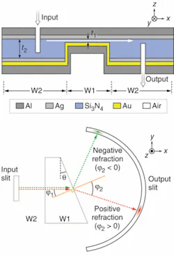
To visualize negative refraction, the experimental setup consists of three cascaded metal-insulator-metal waveguides: the thin Au/Si3N4/Ag waveguide, and thicker Ag/Si3N4/Ag waveguides with 500 nm cores (see figure). Unlike the 50 nm Au/Si3N4/Ag waveguide, the thick Ag/Si3N4/Ag waveguides sustain only positive-index modes for all wavelengths. The thin Au/Si3N4/Ag waveguide is positioned between the thicker Ag/Si3N4/Ag waveguides, and subwavelength slits are used to couple laser light into and out of the waveguides. Moreover, aluminum cladding layers ensure that no laser light leaks into or out of the structure except at the input and output slits.
When the Au/Si3N4/Ag waveguide is shaped into a prism, the refraction angle can be directly observed. Experimentally, a guided mode is launched into the first positive-index waveguide and excites a SPP mode that propagates through the thin Au/Si3N4/Ag waveguide. When this SPP mode encounters the slanted interface between the middle and output metal-insulator-metal waveguides, it refracts according to Snell’s law. Depending on the incident-laser wavelength, negative and positive refractions are recorded and negative indices as large as -5 are achieved.
Additional experiments using prism-shaped waveguides in different configurations confirm the presence of all-angle negative refraction in the blue-green visible wavelength range between 476 and 514 nm. “Direct visualization of negative refraction is a first milestone to realizing two-dimensional superlenses and invisibility cloaks in the visible,” says Jennifer Dionne, one of the researchers. “The inherent simplicity of this structure hints at its potential as a building block for future negative-index media in three dimensions,” adds Henri Lezec, lead author.
REFERENCE
1. H.J. Lezec et al., Science Express 10.1126/science.1139266, 1 (March 22, 2007).
About the Author

Gail Overton
Senior Editor (2004-2020)
Gail has more than 30 years of engineering, marketing, product management, and editorial experience in the photonics and optical communications industry. Before joining the staff at Laser Focus World in 2004, she held many product management and product marketing roles in the fiber-optics industry, most notably at Hughes (El Segundo, CA), GTE Labs (Waltham, MA), Corning (Corning, NY), Photon Kinetics (Beaverton, OR), and Newport Corporation (Irvine, CA). During her marketing career, Gail published articles in WDM Solutions and Sensors magazine and traveled internationally to conduct product and sales training. Gail received her BS degree in physics, with an emphasis in optics, from San Diego State University in San Diego, CA in May 1986.