MICROCAVITY LASERS: Polariton cavity lases at room temperature
Researchers at the University of Southampton (Southampton, England) and the Institute of Quantum Electronics and Photonics (Lausanne, Switzerland) have reported room-temperature operation of a microcavity gallium nitride (GaN) polariton laser with an input-power threshold of only 1 mW, which, at an absorbed energy density of 29 mJ/cm2, is an order of magnitude lower than the best performance obtained to date with optically pumped GaN quantum-well vertical-cavity surface-emitting lasers (VCSELs).1
Because polaritons are bosons (actually composite bosons made of an electron, a hole, and a photon) that can potentially condense into macroscopic coherent states at room temperature (300 K and above), the research results might eventually enable room-temperature, solid-state Bose-Einstein condensates that might be used to construct, for instance, interferometer chips for high-precision measurements, according to Jeremy Baumberg, who directs the nanomaterials facility at Southampton.
A “polariton” (technically referred to as an exciton-polariton because of its half-light, half-matter nature) is formed when a photon emitted by an electron-hole pair within a cavity is reabsorbed back into the same electron-hole pair before interacting with anything else, making it impossible to discriminate between the photon and the electron-hole pair because of the rapid cycling of energy back and forth between them, he said.
In 2000, Baumberg and coworkers observed huge optical nonlinearities and unprecedented levels of optical gain in polaritons within gallium arsenide (GaAs)-based microcavities. The effects occur because bosons, such as polaritons, tend to congregate in the same quantum state, unlike fermions, such as electrons, that do not share the same quantum state at the same time. They demonstrated a potential practical application at the time by building a micron-scale optical parametric oscillator. The practicality was limited, however, because the devices would only operate at low temperatures below 50 K because of the relatively slow rate of emission and absorption in GaAs.
High-quality mirrors
The faster-emitting GaN material system offered a potential for operation above 300 K; after five years of research with GaN, the Southampton researchers and colleagues in the European Union have fabricated a semiconductor microcavity that relies on polariton effects at room temperature. The achievement was due in large part to advances in the growth of high-quality cavity mirrors in GaN alloys at the Institute of Quantum Electronics and Photonics.
In a polariton laser, the processes of stimulation and emission are separated, Baumberg explained. Excited semiconductor states undergo stimulated scattering into the lowest polariton state, where a large population accumulates leading to emission of photons through the cavity mirrors. Because the lasing states do not require a population inversion, however, pumping thresholds can be much lower and are no longer related to the volume of the laser.
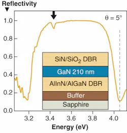
Polariton effects have also been observed in recent work on cadmium telluride quantum-well microcavity lasers, but thermal decoherence obliterates those effects at temperatures above 220 K. Baumberg’s team used bulk GaN microcavities based on a hybrid design to avoid the broad linewidths and quantum-confined Stark effects that are characteristic of nitride-based quantum wells (see figure).
The experimental setup consisted of a UV femtosecond goniometer system enabling both incident pump and emission angles to be scanned over angles up to 80°. Frequency doubling the visible output of an optical parametric amplifier provided a 150 fs spectrally tunable pump pulse, and pump wavelength was scanned initially from 250 to 320 nm while monitoring the emerging photoluminescence. The p-polarized pump pulses were focused to a 60-µm-diameter spot on the top distributed-Bragg-reflector mirror to excite the sample nonresonantly, and resulting emissions were collected through a UV multimode collection fiber leading to a 0.5 m monochromator and liquid-nitrogen-cooled CCD. Polariton effects were observed over a large area of the sample by retuning the pump as necessary to maintain Bragg resonance.
Baumberg emphasized that a lot of work remains before practical possibilities such as interferometers on a chip can be achieved. “The GaN material is still under development, and electrical pumping needs to be developed, though in principle there are no roadblocks for this,” he said. “However, the consistent progress seen over the last seven years indicates the rich potential in basic science and novel technologies awaiting polariton devices.”
REFERENCE
1. S. Christopoulos et al. Phys. Rev. Lett. 98 , 126405 (2007).
About the Author
Hassaun A. Jones-Bey
Senior Editor and Freelance Writer
Hassaun A. Jones-Bey was a senior editor and then freelance writer for Laser Focus World.
