SILICON OPTOELECTRONICS: Unique process creates curvilinear ‘eye’ camera

Researchers at the University of Illinois at Urbana-Champaign (Urbana, IL) and Northwestern University (Evanston, IL) have succeeded in developing the first curvilinear or hemispherically shaped working camera that reduces optical distortions associated with flat-sensor cameras.1 The camera is built from planar silicon optoelectronic components that are formed into an eye-shape nonplanar distributed focal array using a unique and repeatable process.
The camera follows the development of expandable silicon designed to meet large-area applications and a curved silicon sensor array, both at Stanford University, which was reported in the March and June 2008 issues of Laser Focus World (see www.laserfocusworld.com/articles/322010 and www.laserfocusworld.com/articles/330736).
In simple terms, a hemispherically shaped elastomeric form is cast and cured from a liquid prepolymer into a flexible polydimethylsiloxane (PDMS) material. The shape is formed by injecting the uncured polymer into the gap between a convex and concave lens with matching radii of curvature (approximately 1 cm). This hemispherical form with a raised rim is then mounted in a mechanical fixture with ten paddle arms that insert into the rim. By applying radial tension to the arms, the PDMS structure is stretched into a flat “drumhead,” meaning that all points in the flattened PDMS are in biaxial tension.
In a separate conventional process, single-crystalline silicon photodiodes, current-blocking p-n junction diodes, metal interconnects, and polyimide films between the elements and encapsulating the system are formed as a planar focal-plane array on a silicon-on-insulator (SOI) wafer. An acid etch removes the SOI material, leaving a flexible planar structure with individual optoelectronic elements interconnected both mechanically and electrically by the polyimide/metal structures, which act as tiny ribbon-type cables.
Hemispherical shape
This planar array is then placed in contact with the tensioned drumhead PDMS form. When the drumhead tension is removed, the silicon polyimide structure adheres to the PDMS form by van der Waals interactions, and the entire structure is raised back up into a hemispherical shape. The individual silicon optoelectronic elements are essentially compressed and move closer together as the polyimide/metal interconnects buckle into arc-shape structures out of the plane.
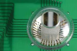
The final steps in the fabrication of this curvilinear eye-shape camera involve attachment of the structure to a matching curved glass substrate using photocurable adhesive and mounting to a printed-circuit board. A hemispherical cap with a simple imaging lens is then placed over the structure, completing the eye camera (see figure).
According to the researchers, the beauty of this method is that the silicon structures and the deformable “ribbon cable” interconnects can be fabricated using conventional planar processes. For this particular camera, a 16 × 16 array of photodiode and p-n junction-blocking diodes with metal interconnects allows capture of visible images.
“These and related strategies might offer opportunities for new classes of imaging systems in which design optimization involves not only the lens configurations but also the detector geometries,” says John A. Rogers, professor of materials science and engineering at the University of Illinois at Urbana-Champaign. “Other opportunities might arise from the ability to integrate electronics and optoelectronics with the curvilinear surfaces of the human body, in important ways that would be inconceivable with conventional, rigid, wafer-based technologies.”
REFERENCE
- H.C. Ko et al., Nature 454, 748 (Aug. 7, 2008).
About the Author

Gail Overton
Senior Editor (2004-2020)
Gail has more than 30 years of engineering, marketing, product management, and editorial experience in the photonics and optical communications industry. Before joining the staff at Laser Focus World in 2004, she held many product management and product marketing roles in the fiber-optics industry, most notably at Hughes (El Segundo, CA), GTE Labs (Waltham, MA), Corning (Corning, NY), Photon Kinetics (Beaverton, OR), and Newport Corporation (Irvine, CA). During her marketing career, Gail published articles in WDM Solutions and Sensors magazine and traveled internationally to conduct product and sales training. Gail received her BS degree in physics, with an emphasis in optics, from San Diego State University in San Diego, CA in May 1986.