ATOM OPTICS: Smooth operator: a quantum-stabilized mirror is ‘smoothest surface ever’

Ultrasmooth mirrors could enable a new kind of microscope: a scanning helium-atom microscope that could use helium (He) particles as nondestructive probes to image nanometer-scale surface details of a material. Such microscopes hold promise for their potential to investigate delicate surfaces such as fragile biological samples without charging or exciting their electrons. But previous attempts to build them using a crystal to focus the helium beam suffered from poor reflectivity of less than 1%.1 Now, scientists at the Autonomous University of Madrid, Spain, have used “quantum size effects” to achieve a focusing mirror with a very high reflectivity for He atoms bounced off its surface–reportedly the “smoothest surface ever.”
The so-called atom mirror uses thin layers of lead (Pb) grown on a thin silicon (Si) wafer. Metals grown on semiconductor surfaces typically form uneven three-dimensional “islands” that prevent them from being used as effective focusing optics for matter waves. But certain ultrathin metal films, when deposited on a substrate with a symmetry gap around the Fermi energy, display a strong quantum confinement of the electrons. This quantum-stabilized surface favors islands of similar heights, which enables its use as an ultrasmooth mirror in “atom optics”–the coherent manipulation of matter waves.
“Magic” thicknesses
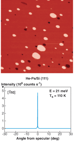
To design the atom mirror, professor Rodolfo Miranda and colleagues deposited between 1 to 18 monolayers (MLs) of Pb on the surfaces of several 50-µm-thick Si(111) wafers in an ultra-high-vacuum chamber. As the film grew, the group charted the scattering of a 2 mm He beam as it demonstrated varying levels of diffraction and reflection. At certain precise “magic” thicknesses, the specular intensity revealed sweet spots. At seven monolayers (ML) thick, for example, the film was atomically flat with 94% of the surface at 7 ML high, with 6% of the surface forming slightly depressed or raised islands (see figure).
This specimen was heated to 260 K (-13°C) to anneal and further flatten the film. The He diffraction spectrum recorded along with [-110] azimuth exhibited reflectivity of up to 15% at an angle of incidence of θi = 51° and an energy of Ei = 28 meV. This intensity is 15 to 20 times higher than that of the Si(111) substrate alone. Modeling predicts that much larger reflectivities as high as 40% could be achieved by optimizing for large angles of incidence and small incident energy.
Bodil Holst, professor at the department of physics and technology at the University of Bergen, Norway, has worked for years on the development of a helium-atom microscope as part of the Imaging with Neutral Atoms consortium along with the Madrid group. She and her group recently used a zone-plate mechanism to achieve transmission images with a resolution of 2 µm, and will soon announce submicron resolution, but such images suffer from chromatic aberration.2 If Miranda and his team’s atomic mirror can focus the beam to a bright-enough intensity, and the surface of the mirror can be successfully bent, the next step would be to incorporate it into a new helium microscope.
“The big achievement of Miranda et al. was to apply a new coating to the silicon surface, which yielded a specular reflectivity of 20% or more,” says Holst. “At the moment, we are designing a new helium microscope that will produce images in reflection with submicron resolution. We expect to see the first images next year.”
REFERENCES
- D. Barredo et al., Adv. Matls. 20 (18), 3492 (Aug. 2008).
- M. Koch et al., J. Microscopy 229, 1 ( 2008).

Valerie Coffey-Rosich | Contributing Editor
Valerie Coffey-Rosich is a freelance science and technology writer and editor and a contributing editor for Laser Focus World; she previously served as an Associate Technical Editor (2000-2003) and a Senior Technical Editor (2007-2008) for Laser Focus World.
Valerie holds a BS in physics from the University of Nevada, Reno, and an MA in astronomy from Boston University. She specializes in editing and writing about optics, photonics, astronomy, and physics in academic, reference, and business-to-business publications. In addition to Laser Focus World, her work has appeared online and in print for clients such as the American Institute of Physics, American Heritage Dictionary, BioPhotonics, Encyclopedia Britannica, EuroPhotonics, the Optical Society of America, Photonics Focus, Photonics Spectra, Sky & Telescope, and many others. She is based in Palm Springs, California.