Daniel Herrmann and Ying Zhou
Light-emitting diodes (LEDs) appear in everything from display technologies such as flat-panel computer displays to light sources like traffic lights and flashlights. Future demands for these applications will require devices capable of producing more light at a lower manufacturing cost and operating power. These new LEDs will not only be brighter light sources, they will be more economical to operate and generate less heat, not to mention smaller and easier to incorporate into other technologies.
One of the largest barriers to achieving a higher-efficiency LED is total reflection within the device; the majority of photons generated are not emitted from the device.1 The disparity is due to the interface between the high-index semiconductor regions of the device where the photons are produced and the lower-index regions that surround it. Computer-based modeling and simulation can be used to investigate methods to circumvent this inefficiency. Specifically, roughening the surface of the LED using diffractive surface gratings such as two-dimensional (2-D) photonic-crystal patterns enables the successful extraction of additional energy from the device.2, 3 To accomplish this, software is required to optimize the parameters of the photonic crystal.
The need to accurately model photonic-crystal patterns at material interfaces translates into a need for suitably rigorous simulation algorithms; nanostructured interfaces require simulation tools that account for physical effects such as diffraction. Two such algorithms are the rigorous coupled-wave analysis (RCWA) and finite-difference time-domain (FDTD) methods.4, 5 These algorithms provide full-vector solutions to Maxwell’s equations and correctly model the diffractive field effects at patterned surfaces. They each provide complementary views of device performance and together yield a more complete picture of device operation. The RCWA method is used to provide a quick understanding of how different geometries perform and FDTD is used to calculate the extraction efficiency of a particular geometry.
Optimizing geometry
To determine how effectively a particular photonic-crystal geometry will improve the extraction efficiency of an LED, the optical engineer must understand the geometry of light transmission over a wide range of incident angles. A nonpatterned flat interface will only allow light incident at angles smaller than the critical angle to be transmitted; light incident at larger angles will be trapped within the device.
We modeled the efficiency of a gallium nitride (GaN)-based LED with a square-lattice photonic crystal. The GaN-based LED structure consists of an interface between the high-index GaN material and air (see Fig. 1). The interface is modified with a square photonic-crystal lattice with a variable period. We modeled a single unit cell of this device using RCWA with periodic boundary conditions and a plane-wave excitation to study how the presence of the photonic crystal affects the angles at which light is coupled out of the device. This structure does allow light at angles greater than the critical angle (about 20° in this case) to be coupled out of the device, which means a higher extraction efficiency. Knowing the angular radiation pattern of the LED light source, we can estimate the extraction efficiency of the photons in this device. However, in practice, this can be tricky since the radiation pattern is hard to determine.
FIGURE 1. In an FDTD simulation, a portion of the electromagnetic field (red, white, and blue area) moves through the GaN-based LED structure, which consists of a high-index GaN material and a photonic-crystal lattice.
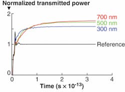
To study this structure in more detail, we required a more realistic simulation model such as the FDTD algorithm. The FDTD algorithm is a general-purpose electromagnetic solver that is ideal for this type of 3-D computation. The FDTD algorithm can incorporate a nonuniform grid, allowing for additional grid points to be used near material interfaces where fields tend to change rapidly. The FDTD algorithm also lends itself to distributed calculations in which the simulation workload is spread across several computers on a network to result in faster and larger simulations. To correctly simulate the incoherent nature of light from the active region of the LED, we placed a 2-D layer of dipole sources beneath the photonic-crystal surface; each dipole continuously driven in time at the same frequency. These dipole sources were given a random phase and orientation pointing along the active layer. Perfectly matched layer conditions were used at the domain edges, allowing electromagnetic energy to leave the simulation domain without reflection. To determine the extraction efficiency of the LED, we measured the transmitted power (see Fig. 2). These results represent an integration of the normal component of the Poynting vector measured in a plane that lies outside the LED. Several results are shown for various photonic-crystal periodicities. Note that the results have been normalized such that the reference result, which was obtained by simulating without a photonic crystal, equals unity.
This simple example saw a modest increase in output power; a finely tuned lattice can produce even better results. Simulation tools provided a quick and easy way to quickly explore the design parameter space to determine optimal design parameters. The inclusion of a metallic reflector behind the active region further increased the efficiency. Furthermore, though not examined here, the use of a photonic-crystal layer can modify the radiation pattern of the LED and assist in creating better directional sources of light. The search for more efficient LED devices requires simulation tools capable of accurately modeling physical field effects such as diffraction.
REFERENCES
1. J-Y. Kim et al., Appl. Phys. Lett. 91, 181109 (2007).
2. W. J. Choi et al., Journal of the Korean Physical Soc. 49, 877 (2006).
3. L. B. Chang, IEEE Phot. Tech. Lett. 91, 1175 (2007).
4. M. G. Moharam et al., J. Opt. Soc. Am. A 3, 1780 (1986).
5. A. Tavlove, Computational Electrodynamics: The Finite-Difference Time-Domain Method, Artech House, Norwood, MA (1995).
Tell us what you think about this article. Send an e-mail to [email protected].
DANIEL HERRMANN and YING ZHOU are application engineers at RSoft Design Group, 400 Executive Blvd., Suite 100, Ossining, NY 10562; e-mail: [email protected]; www.rsoftdesign.com.

