OPTOELECTRONIC APPLICATIONS: DNA PHOTONICS - Next-generation optoelectronics leverage DNA biopolymers
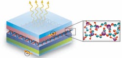
Deoxyribonucleic acid (DNA)—the magic double helix that is the blueprint of different life forms on Earth—is working its way into a new kind of laboratory. In addition to its use in genetic mapping, cloning, disease understanding and prevention, and crime-scene investigation being exploited in medical laboratories, DNA is now appearing in clean rooms of semiconductor and thin-film coating facilities. It turns out that DNA, when concentrated into a thin-film biopolymer through reactions with surfactants, can be used to create improved optoelectronic devices (see Fig. 1).
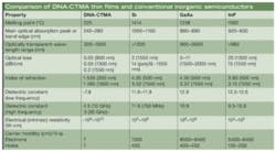
“While the optical properties of DNA biopolymer films can be neatly listed in a table and easily measured in terms of optical absorption, reflectance, transmission, and thermal stability, there is still a great deal of art that goes into creating the thin films to begin with,” says Andrew Steckl, Gieringer Professor and Ohio Eminent Scholar at the University of Cincinnati NanoLab (Cincinnati, OH). Moving DNA biopolymer from an art form into a commercially viable material is the goal of researchers like Steckl, who is attracted by the fundamental optical and electrical properties of DNA biopolymer thin films—properties that are very appealing when compared to other polymers; and in certain aspects, even to some common semiconductor materials (see table).1Why DNA?
“These DNA-based materials possess unique electromagnetic and optical properties that no other known polymers have: low optical loss over a broad wavelength (350 to 2000 nm) and five orders of magnitude more conductivity,” says James G. Grote, principal electronics research engineer at the Air Force Research Laboratory Materials and Manufacturing Directorate (Wright-Patterson Air Force Base, OH).
Grote began working with DNA in 2000 after attending a seminar given by professor Naoya Ogata of the Chitose Institute of Science and Technology (CIST; Hokkaido, Japan). “I was working on conductive cladding materials for nonlinear-optic (NLO) polymer electro-optic modulators at the time; problem was, when a material with acceptable optical loss and conductivity was realized, these polymers typically used the same solvent as the NLO polymer core material so the various layers would dissolve each other,” says Grote. “The purified DNA that Ogata had developed was insoluble in those same organic solvents, and so my work began.”
While on sabbatical at USC, UCLA, and the University of Washington in 2001, Grote worked with professors Larry Dalton, Harold Fetterman, William Steier, and Alex Jen to develop the initial processing steps for DNA biopolymers—an ongoing area of study for several researchers (see “Turning DNA into a thin-film polymer,” p. 70). “The dielectric constant of DNA is tuned with an applied electric field with the same amount of tunability as the ferroelectric barium strontium titanate (BST), but can be simply spin deposited, while BST needs to be grown at high temperature,” says Grote. “In addition to spin depositing, casting, and flow coating, DNA can also be vapor deposited, pulsed-laser deposited, and ink-jet printed. Furthermore, DNA is nonfossil-fuel-based—a “green” product derived from waste, biodegradable, abundant, replenishable, and inexpensive.”2
But for all the accolades and research aimed at DNA photonics, the technology still evokes a certain criticism. “A report published some 15 years ago showed that the nonlinear optical properties of wet DNA films are much less expressed when the water content is low, probably because the DNA structure is disordered at low humidities,” says Jewgeni Starikow of the Institute for Nanotechnology, Research Center of Karlsruhe, Germany, who has worked on DNA physical chemistry for 25 years.3 “Even the linear optical response of DNA is not yet well understood.4, 5 This casts doubts on whether the observed effects are due to DNA itself.”
Still, research groups around the world are forging ahead in several application areas, recognizing that “green” photonic solutions with interesting optoelectronic properties such as DNA biopolymers merit further research.
Illumination and displays
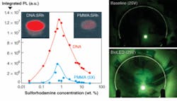
Andrew Steckl and colleagues at the University of Cincinnati have used DNA to improve the efficiency of organic light-emitting diodes (OLEDs) for illumination and displays. First, a DNA-based thin-film polymer is created using DNA and cetyltrimethylammonium chloride (CTMA-Cl) in a cationic surfactant reaction to create a DNA-CTMA complex. When incorporating this electron-blocking thin-film DNA-CTMA layer into a standard 2 × 2 mm active-area OLED design, the luminous efficiency of the resultant DNA-based “BioLED” is two to ten times better than OLEDs that use no blocking layer or conventional polymethylmethacrylate (PMMA) or polyvinyl carbazole (PVK) blocking layers (see Fig. 2).6 “By adding a stilbene-type fluorescent dye to DNA we discovered that the photoluminescence we measured was 100 times greater than the amorphous polymers typically used,” says Grote.Steckl’s team also investigated DNA as a host material for optically pumped organic solid-state lasers.7 In a distributed-feedback laser structure, sulforhodamine 640 (SRh)-doped DNA stimulated emission had a threshold energy that was approximately twice as low as a corresponding PMMA:SRh structure and a slope efficiency that was approximately twice as high.
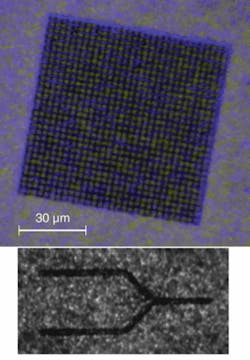
For two-photon excited upconversion lasing, Paras Prasad, distinguished professor and executive director of the Institute for Lasers, Photonics and Biophotonics at the University at Buffalo, is exploring DNA as a solid-state medium in which strong two-photon absorbing dyes can be incorporated in high loading density without aggregation. His group has demonstrated very efficient upconversion lasing of a dye-doped DNA medium, and has also prepared high-optical-quality nanocomposites of DNA and organically modified silica, useful for light-guiding components (see Fig. 3).8, 9Grote’s early modulator work continues at the University of Dayton (Dayton, OH) with professors Perry Yaney, Guru Subramanyam, and Liming Dai, who have also demonstrated DNA-CTMA complex as a hole-transporting/electron-blocking layer in multilayer (up to five layers) white polymer OLEDs that achieve high brightness (10500 cd/m2) and improved white-color stability.10
Information processing and sensing
A team led by professor Richard Kiehl at the University of California at Davis is exploring optoelectronic devices based on the structural properties of DNA by focusing on plasmonics in metallic nanoparticle arrays that are self-assembled into a two-dimensional DNA scaffolding.11 “Plasmonic interactions (certain electric dipole interactions) between metallic nanoparticles are critical in the emerging field of ‘nanophotonics,’ where waveguiding of light can be achieved with structures much smaller than the free-space optical wavelength,” says Kiehl. “In our work, DNA is used as a passive scaffolding that directs the self-assembly of nanoparticles into 1-D and 2-D arrays with extreme precision at nanoscale dimensions. What’s more, the position, size, and type of the nanoparticles can be precisely ‘programmed’ by the DNA base-sequence design to allow systematic studies of plasmonic interactions in complex structures at size regimes not possible by other techniques.”
Kiehl projects that applications of these DNA-assembled nanophotonic structures will include signal processing and information processing at the nanoscale; in addition, the natural ability to precisely assemble organic and inorganic nanocomponents within the same structure by this technique could offer new optical approaches to chemical and biochemical sensing.
Other photonics applications
Francois Kajzar at the University of Angers in France is developing DNA-based third-order nonlinear materials for holographic applications; professors Marek and Anna Samoc at The Australian National University experiment with DNA-based metamaterials; and professor Ileana Rau at the Polytechnic University of Bucharest studies DNA-based organic dyes for optical applications. And in a more futuristic application, professor Birendra Singh and director Serdar Sariciftci of the Linz Institute for Organic Solar Cells at Johannes Kepler University (Linz, Austria) envision DNA complexes being used for bio-organic cybernetics. “The compatibility of carbon/hydrogen-based DNA organic semiconductors with organic biomolecules creates a great opportunity for integration with living organisms,” Singh says.
“There is a lot of potential for this new DNA photonics field,” says Grote. “In addition to being used for genomic sequencing and clinical diagnosis and treatment, DNA is well on its way to being thought of as a commercial product.”
REFERENCES
1. A.J. Steckl, Nature Photonics 1(1) 3 (January 2007).
2. J.G. Grote, SPIE Nanotechnology Newsroom, 10.1117/2.1200805.1082 (May 2008).
3. W. Williamson III et al., Spectroscopy Lett. 26 (5) 849 (1993).
4. D. Markovitsi et al., Nature 448, E7 (June 8, 2006).
5. C.E. Crespo-Hernández et al., Nature 448, E8 (June 8, 2006).
6. J.A. Hagen et al., App. Phys. Lett. 88, 171109 (April 24, 2006).
7. Z. Yu et al., Appl. Optics 46(9) 1507 (March 20, 2007).
8. G.S. He et al., Optics Lett. 31(3) 359 (2006).
9. P. Gupta et al., Appl. Phys. Lett. 88, 213109 (2006).
10. Q. Sun et al., Appl. Phys. Lett. 92, 251108 (2008).
11. Y.Y. Pinto et al., Nanotechnology Lett. 4, 2399 (2005).
Turning DNA into a thin-film polymer
To make efficient biopolymers, a better understanding is needed of the chemical composition of the DNA material as it is synthesized from its low-density water environment to a dryer, condensed state. “DNA’s natural environment is water, but 99% of the [optoelectronic] devices we work on are solid-state,” says Andrew Steckl. While DNA in solution is being explored for use in optofluidic devices, Steckl sees three critical areas of research necessary to establish the commercial viability of DNA biopolymer-based photonic devices: ensuring an adequate material supply, perfecting the conversion from water-soluble to organic-solvent-soluble DNA, and controlling the “wet-to-dry” transition and understanding its effect on the DNA structure and properties.
Adequate supply of DNA material is now becoming possible, thanks to collaborations between photonics researchers and commercial fishing and farming industries. “Synthetic DNA is not plentiful—we cannot get by with micrograms of material; we need grams upon grams and a stable supply,” says Steckl. Steckl relies on his supply of DNA from salmon sperm, a biowaste product of the salmon fishing industry, and now made available through a collaborative effort between CIST, the Asian Office of Aerospace Research and Development (Tokyo, Japan), and the AFRL/RX. Steckl is also starting to look at salmon-sperm DNA from farm-raised salmon through Biokom (Puerto Montt, Chile), and notes that DNA from different sources has different molecular weights. Grote and his collaborators are also investigating plasmid DNA grown from bacteria where the molecular weight, protein content, and even the sequence can be controlled more economically than synthetic DNA, and on a much larger scale.
Removing water from DNA in solution, the form in which it arrives to the laboratory, remains a critical step in the DNA biopolymer synthesis process. Currently, DNA thin films are produced by solution methods in which a reaction between the DNA and a cationic surfactant creates a DNA-lipid complex that is insoluble in water, but soluble in alcohols. Water insolubility is crucial when building optoelectronic devices comprised of layers of different materials that require cleaning with water between various fabrication steps.
Fabricating water-insoluble DNA thin films—either by solution methods or by ultrahigh-vacuum molecular-beam deposition in a dry process—is a complex process that aims for the subsequent casted or spin-coated films of DNA to have stable and reproducible optical and electrical properties.1 For example, researchers have found that reducing the starting DNA molecular weight significantly decreases the electrical resistivity of the DNA film, which can be critical for the fabrication of some optoelectronic devices.
REFERENCE
1. J. Hagen et al., Nano Lett. online, 10.1021/n1062342u (Dec. 1, 2006).

Gail Overton | Senior Editor (2004-2020)
Gail has more than 30 years of engineering, marketing, product management, and editorial experience in the photonics and optical communications industry. Before joining the staff at Laser Focus World in 2004, she held many product management and product marketing roles in the fiber-optics industry, most notably at Hughes (El Segundo, CA), GTE Labs (Waltham, MA), Corning (Corning, NY), Photon Kinetics (Beaverton, OR), and Newport Corporation (Irvine, CA). During her marketing career, Gail published articles in WDM Solutions and Sensors magazine and traveled internationally to conduct product and sales training. Gail received her BS degree in physics, with an emphasis in optics, from San Diego State University in San Diego, CA in May 1986.


