BEAM SHAPING: Plasmonics squeeze IR light into nanospot
Coupling light into a nanoscale spot is extremely important to applications in high-density optical interconnection, sensitive modulators, optical data storage, nanostructure manipulation, and lithography. To date, efforts to accomplish this have been very inefficient or achieve efficient coupling in only one dimension. But by leveraging prior demonstrations using nanoscale structures and surface-plasmon polaritons (SPPs), researchers at the Rochester Institute of Technology (RIT; Rochester, NY) have successfully squeezed a 1550 nm infrared (IR) beam into a 21 × 24 nm spot with 62% efficiency.1
Previous coupling demonstrations have successfully channeled 532 nm light along a 250-nm-long silver waveguide strip with a 250 × 50 nm cross section. And nanowire tapers and planar tapers have been reported that channel light along their surface by converting photons into SPPs. However, these methods are usually inefficient due to scattering and coupling losses, perform deep subwavelength coupling only in one dimension, and typically involve complex optical setups.
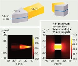
One method of increasing efficiency is to couple light from a dielectric waveguide into a metal-dielectric-metal (MDM) plasmonic waveguide. Extending this concept further, the researchers used the efficient coupling between a dielectric waveguide and an MDM plasmonic waveguide to shrink the vertical dimension of the beam, and then coupled this light into a tapered MDM waveguide to shrink the horizontal component (see figure).
To determine the optimum physical and optical parameters of the dielectric waveguide and the tapered MDM plasmonic waveguide, three-dimensional (3-D) finite-difference time-domain (FDTD) simulations using 1550 nm light were performed. The silicon dielectric waveguide has a width of 320 nm and a height of 300 nm, while the tapered MDM waveguide has a slightly larger cross section at 400 × 400 nm, 550 nm length, and consists of a 20-nm-thick silicon dioxide plasmonic waveguide sandwiched between two silver slabs. Inserted between the dielectric waveguide and the MDM waveguide is a rectangular (nontapered) 50-nm-thick section of MDM waveguide used as a buffer.
Once light is incident on the interface between the dielectric waveguide and MDM plasmonic waveguide, surface plasmons are excited and they can be funneled like a liquid into the dielectric part of the plasmonic waveguides. The taper in the horizontal direction then squeezes light in the other direction.
Large electric-field enhancement
Infrared (1550 nm) light input to the first dielectric has mode-field dimensions of approximately 232 × 156 nm. As light propagates toward the MDM taper tip, the power density becomes progressively stronger. Taking into account an estimated 18% loss due to back-reflection at the MDM taper interface and a 20% loss due to transverse scattering at the interface and propagation loss in the MDM plasmonic taper, efficiency is roughly 62% at the 21 × 24 nm output. Such tight horizontal and vertical squeezing also results in an electric-field enhancement of 31× at the output port.
Although shorter tapers could reduce the propagation losses, back-reflection losses would correspondingly increase.
“The mode size that light can be confined in a dielectric waveguide and the spot size that light can be focused by a lens are restricted by the diffraction limit, which is roughly about 0.5 λ, or approximately 800 nm at telecom wavelengths,” says Zhaolin Lu, assistant professor of microsystems engineering at RIT. “The large focused spot limits the capacity of data-storage media, while the large mode size restricts the optical integration density and even worse, gives rise to dimension mismatch between electronic devices (with feature size of approximately 50 nm) and photonic devices. Plasmonic waveguides support nanoscale modes with acceptable propagation loss and are believed to be the technique merging photonics and electronics at nanoscale dimensions. In this sense, nanoscale confinement of light is the initial motivation to develop surface plasmon-based circuits. A key feature of our device is that it is a planar structure and can be fabricated with standard semiconductor techniques.”
He notes that his group is looking into experimental demonstrations of various applications, particularly in high-speed all-optical signal processing and optical interconnection.
REFERENCE
- R.Yang et al., Optics Express 16(24) p. 20142 (Nov. 24, 2008).

Gail Overton | Senior Editor (2004-2020)
Gail has more than 30 years of engineering, marketing, product management, and editorial experience in the photonics and optical communications industry. Before joining the staff at Laser Focus World in 2004, she held many product management and product marketing roles in the fiber-optics industry, most notably at Hughes (El Segundo, CA), GTE Labs (Waltham, MA), Corning (Corning, NY), Photon Kinetics (Beaverton, OR), and Newport Corporation (Irvine, CA). During her marketing career, Gail published articles in WDM Solutions and Sensors magazine and traveled internationally to conduct product and sales training. Gail received her BS degree in physics, with an emphasis in optics, from San Diego State University in San Diego, CA in May 1986.
