METAMATERIALS: Fishnet structure has negative index in yellow light

For the first time, researchers have created a negative-refractive-index optical metamaterial that operates in the yellow portion of the visible spectrum (580 nm).1 Previously, the shortest wavelength at which such a material could be made to operate was at 715 nm, in the red region.2
Optical metamaterials, which are periodic subwavelength-size structures of noble metals and dielectrics, have been around for almost 10 years and have allowed the fabrication of “superlenses” that focus far-field and evanescent waves to image at below the diffraction limit, as well as rather crude forms of “invisibility cloaks,” which distort the electromagnetic field around objects so as to hide them (some simulations of cloaking have been spectacular, creating popular perceptions that are almost impossible for experimental results to live up to).
Superlenses have many potential uses in biological sensing and imaging, so the pushing of metamaterial operating wavelengths from the red to the yellow region, and sooner or later to blue, will open up practical applications. Efforts are also going into improving the transmission of metamaterials.
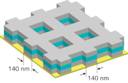
The yellow-light metamaterial was developed by a group at Purdue University (West Lafayette, IN). One challenge is to fabricate a metamaterial structure that is fine enough and accurate enough in form to be functional. The Purdue researchers decided on a so-called fishnet structure design, which had previously been used experimentally and appeared to be scalable to smaller size (see figure).
A finite-element simulation, including fabrication constraints, resulted in an optimum unit-cell size of about 220 nm in both the electric- and magnetic-field vector directions (the two lateral surface directions) and a metal coverage of about 70%. From top to bottom, the layers were 10 nm of aluminum oxide (Al2O3), 43 nm of silver (Ag), 45 nm Al2O3, 43 nm Ag, 10 nm Al2O3, and the glass substrate.
The structure was fabricated via electron-beam writing. While the voids in the design had perfectly sharp corners, the fabricated structure had rounded voids–a result of electrons backscattering during writing.
The metamaterial was optically characterized using normal-incidence polarized light; two dips in reflection were observed: at 570 and 526 nm. The longer-wavelength dip arose from the material’s magnetic resonance, while the other dip arose from the electric resonance. The theoretical and experimental transmittance and reflectance spectra matched very closely, giving the researchers confidence that they could calculate the effective refractive index.
The result was a negative refractive index for one polarization in the range between 567 and 602 nm, with the lowest index at 580 nm, where it reached -0.25. The negative index resulted from a negative permittivity and a positive permeability, which makes the material a “single-negative” metamaterial. The figure of merit for the material, which is a measure of its optical loss, was 0.3 at 580 nm (the higher the number the better; 0.3 is not particularly low-loss, but then this was the first yellow-light metamaterial ever made).
A “double-negative” metamaterial–negative in permittivity and permeability–would be the next step, as it would widen the range of optical elements that could be created.
REFERENCES
1. S. Xiao et al., Optics Lett. 34(22) (Nov. 15, 2009).
2. G. Dolling et al., Optics Lett. 32(53) (2007).
About the Author
John Wallace
Senior Technical Editor (1998-2022)
John Wallace was with Laser Focus World for nearly 25 years, retiring in late June 2022. He obtained a bachelor's degree in mechanical engineering and physics at Rutgers University and a master's in optical engineering at the University of Rochester. Before becoming an editor, John worked as an engineer at RCA, Exxon, Eastman Kodak, and GCA Corporation.
