OPTICAL FABRICATION: Advances in sputtering benefit coating costs
IAIN MACMILLAN
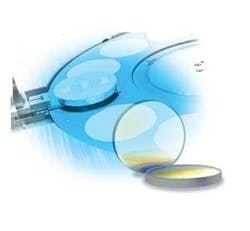
As the number of optical applications in the life sciences, military, and laser optic industries continues to grow, the demands on optical coatings extend to designs of increasing complexity with tighter tolerances. In concert with these requirements comes the need for greater throughput and higher yields, thus setting the goal of increasing volume with better performance at lower cost (see Fig. 1).
High-precision optical coatings for these demanding applications have historically been deposited by the preferred method of evaporation but have proved problematic to manufacture. In comparison to less complex products like antireflection coatings, high-precision coatings produced by evaporation are subject to lower yields, reduced capacity, and can require several additional fabrication steps after coating. Hard-oxide evaporated coatings require lengthy production cycles. Coatings using sulphide/fluoride combinations deposit faster than hard oxides, use fewer layers, and coat at lower temperatures, resulting in shorter production cycles. However, these coatings are less durable, are moisture sensitive, and need to be encapsulated and protected from environmental exposure. Capacity, yield, production-cycle time, and added fabrication steps all are significant cost drivers–unfortunately for evaporation technology, they are driving in the wrong direction.
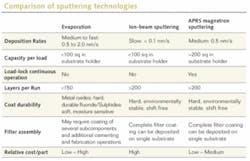
The emergence of ion-beam-sputtering (IBS) technology in the 1970s led to development of very-low-loss, stable, shift-free optical coatings (see “Evaporation vs. sputtering”). These coatings exhibited very low absorption and scatter from multiple layers constructed of tantalum pentoxide and silicon dioxide. Ion-beam sputtering found a market in specialized applications such as ring-laser gyroscopes, and in the 1990s IBS was at the forefront of filter development for dense wavelength-division multiplexing, in which the low-loss stable coatings advanced narrowband filter capability to new levels. Despite its advantages, however, only a few companies in North America adopted IBS as their core coating technology. Factors working against IBS included high capital investment (more than $1 million per machine), low deposition rates (resulting in very long production cycle times), and relatively small capacity per chamber batch. The net result was a high cost-per-unit coated part.
During the past decade, high-end coating manufacturers have been seeking a technology solution that would provide much of the control and properties of IBS films but with significantly reduced cost per coated part–closer to that of evaporation costs. Many firms have developed their own technologies. For the most part, these technologies are based on sputtering of metals with subsequent oxidation at the substrate surface. The processes use a combination of magnetrons, ion guns, and/or plasma sources although details are generally unavailable because of the proprietary nature of this equipment.
More recently, advances in sputtering technology have resulted in coating equipment capable of producing complex optical coatings of more than 200 layers. In one example, advanced plasma reactive sputtering (APRS) uses mid-frequency dual-magnetrons and achieves consistent, repeatable rates of deposition with highly predictable thin-film optical characteristics. Armed with accurate optical and time-based layer monitoring techniques, APRS is capable of producing complex filters with spectral performance that closely matches theoretical models.
A few equipment manufacturers have started supplying magnetron-based optical-coating systems. One commercial system, Leybold’s Helios, comes with two dual magnetron sources operating at mid-frequency, which allows deposition of alternating layers of high and low refractive index with complex designs of several hundred layers. Substrates are mounted in 100-mm-diameter holders, which are in turn placed on a turntable. The turntable can hold up to 16 100-mm-diameter holders in one coating run–a relatively large capacity for high-precision coatings. The turntable rotates at speeds of up to 250 rotations per minute. As it rotates, metals are sputtered onto the substrates from each source. Oxidation of the metal layers is completed when the substrates pass through an oxygen plasma located along the path of the turntable rotation, but separated from the magnetron sources. Because the sputtering of metals and the final oxidation process are separated, the metal targets are not prone to charge build-up effects from oxidation of the target, which can be problematic in sputter deposition of metal oxide films. The sputtering of metal targets also enables relatively high deposition rates, close to that of evaporation.So while APRS and IBS produce comparable spectral quality, the slower deposition times (longer production cycles) of IBS and reduced capacity result in a higher cost per piece using IBS (see table). Evaporated coatings can be deposited at rates equal to or greater than sputtering, however the need to combine several evaporated coatings to produce a single filter assembly along with low yields and reduced capacity at the critical filter stage can raise the unit price for a complex filter. And, while evaporation technology is capable of producing workable filters, the inherent process variations create random errors in layers that result in spectral performance not as close in agreement to theory as either APRS or IBS.
Applications
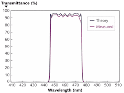
Growth markets for high-precision coatings include biophotonics, military, and laser optics. In biophotonics, the demand for high-precision filters for fluorescence continues to grow, with an emphasis on separation of excitation and emission wavelengths. These filters must exhibit a fast spectral transition from high transmission in the passband to optical-density attenuation levels typically greater than six. This creates signal/noise transmission/blocking ratios of greater than 1 million: 1. Many fluorescence filter designs are based on multicavity bandpass designs of typically 100 to 200 layer construction. To achieve the necessary accuracy during deposition, the filters rely on single-wavelength optical monitoring of turning points in transmission, a method that automatically compensates for thickness errors in previous layers.For layers that show little change in optical response with increasing thickness, such as the coupling layers between cavities, reliable nonoptical methods of monitoring the thickness are required. Multilayers by evaporation are subject to greater random and systematic errors than those from sputtering processes. Changes in process variables such as vapor distribution, rate of deposition, vacuum pressure, temperature, and so forth, throughout the duration of a coating run are more evident in evaporation processes than in sputtering. Layer-to-layer errors are therefore greater in an evaporation process and result in poorer spectral performance than sputtering. Advanced plasma reactive sputtering can successfully produce a 113-layer bandpass filter– typical of a biophotonics-type specification–with measured performance very close to that of the theoretical model (see Fig. 2). In military applications, instrumentation displays, and visual and night-vision sighting systems place increasing demands on coatings either to reject laser radiation while retaining high visible transmission or to balance visible instrumentation display lighting with high-gain near-infrared night-vision illumination.
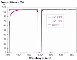
In the former instance, narrowband reflectors, commonly known as notch filters, are used to reflect a specific and potentially destructive laser wavelength while retaining a high level of visible or out-of-band transmission. Notch filters, until recently, have only been successfully manufactured using rugate technology, in which the coating design consists of one layer of sinusoidally changing refractive index instead of the traditional structure of multiple discrete dielectric layers of alternating high and low refractive index.Spectral performance comparable to rugate types can be designed using regular high- and low-refractive-index layers but many of the layers are extremely thin, at less than 10 nm physical thickness. Deposition of such thin layers by evaporation does not produce homogeneous or repeatable results. Thin-layer notch designs manufactured using APRS, however, show excellent agreement with theory, demonstrating the capability of APRS to deposit thin dielectric layers with repeatable and predictable results (see Fig. 3).
In the laser industry, fast-pulse systems such as femtosecond lasers create a new challenge for thin-film designers and coating-process engineers. Specialized coatings must compensate for pulse broadening and chromatic-dispersion effects introduced from multiple reflections occurring within the structure of the multilayer coating. Chirped mirrors are designed to correct these effects but require very low errors in the deposition of the layers. Production of chirped mirrors by evaporation results in low yields because of relatively high random errors from layer to layer. Initial tests using APRS demonstrate improvements in performance compared to evaporation.
Looking forward, as equipment manufacturers develop and introduce larger-volume magnetron systems, it will be interesting to see if this technology platform grows beyond the exclusive high-precision markets. The advantages of repeatable high yields and load-lock continuous operation may make magnetron sputtering a profitable alternative to evaporation even in the medium to low precision markets.
Iain Macmillan is corporate director, optical coatings at Edmund Optics, 101 E. Gloucester Pike Barrington, NJ 08007-1380; e-mail: [email protected]; www.edmundoptics.com.


