MULTISPECTRAL IMAGING: Filter-based multispectral imager has low complexity and cost
By using patterned dichroic filters fabricated with combined thin-film and lithography techniques and a CCD or CMOS sensor architecture, Ocean Optics (Dunedin, FL) and Ocean Thin Films (Largo, FL) have developed a scalable, megapixel multispectral imager that lends itself to low-cost, high-volume multispectral imaging applications.1
Batch-processed filters
Typically, multispectral cameras contain either rotating filter wheels or mechanically diced thin-film dichroic filters mounted in front of an image sensor. Other conventional multispectral systems utilize multiple cameras with bulk dichroic filters or multiple bandpass filters on top of traditional color cameras to image a scene over 4 to 20 different wavelengths.
Color cameras typically use a filtering method in which different-colored gel filters (typically a Bayer pattern with red, green, and blue) are placed over a two-dimensional detector array to create the color camera. The new megapixel multispectral imager uses the same concept, but instead replaces the broad-spectrum colored gels with dichroic filters that capture particular wavelength bands with passbands from 20 to 200 nm. In addition, individual pixels can be long-pass or short-pass filters or optically clear.
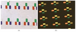
The manufacturing process uses thin-film fabrication methods combined with standard photolithography techniques to essentially pattern thousand or millions of very small (10 µm features with 1 µm registration tolerance to adjacent features) thin-film dichroic filter elements that overlay on top of the pixels in a megapixel array (see figure). The microfilters are made by applying a standard photoresist to a substrate and repeating a series of mask-alignment, exposure, etching, thin film deposition, and lift-off processes to create the filter array. The filters can then be mounted directly onto CCD or CMOS detector arrays.
Because the image is captured in a single shot, spectral and spatial data are gathered simultaneously, with little loss of spatial resolution considering that the array can be of megapixel dimensions. As with off-the-shelf digital cameras, advanced recursive algorithms can interpolate spatial content among different-wavelength pixels to produce high-resolution images in a particular wavelength band.
While the manufacturing process is not practical or cost-effective for someone wanting five systems, it scales well for megapixel imagers when large numbers of systems are needed. “Lower-cost multispectral imagers offer great potential to save lives by helping ensure food safety by scanning produce for contaminants such as in the recent e-coli outbreaks in tomatoes and spinach or helping to identify and define cancer cells during surgery,” says Jason Eichenholz, chief technical officer for Ocean Optics. “While there are hyperspectral systems being developed in research labs for these applications, they are too costly, bulky, and complicated for true widespread deployment. The economies of scale of our coating process make it easy to utilize our multispectral imagers at the supermarket, at a patient’s bedside, on an average farmer’s tractor, or at a packing house.”
REFERENCE
- J.M. Eichenholz and J. Dougherty, Photonics West 2009, OPTO conference paper 7218-40, San Jose, CA (Jan. 28, 2009).

Gail Overton | Senior Editor (2004-2020)
Gail has more than 30 years of engineering, marketing, product management, and editorial experience in the photonics and optical communications industry. Before joining the staff at Laser Focus World in 2004, she held many product management and product marketing roles in the fiber-optics industry, most notably at Hughes (El Segundo, CA), GTE Labs (Waltham, MA), Corning (Corning, NY), Photon Kinetics (Beaverton, OR), and Newport Corporation (Irvine, CA). During her marketing career, Gail published articles in WDM Solutions and Sensors magazine and traveled internationally to conduct product and sales training. Gail received her BS degree in physics, with an emphasis in optics, from San Diego State University in San Diego, CA in May 1986.
