JAMES E. CAREY and JASON SICKLER
The need for inexpensive infrared (IR) light detectors in the commercial, medical, and defense industries is driving rapid development of new IR sensing materials and architectures.1 While there are high-performance material systems for detecting wavelengths in the IR, such as indium gallium arsenide (InGaAs) and mercury cadmium telluride (HgCdTe), these systems are expensive, suffer from reliability issues, and often require additional operating complexity (for example, cooling).
Alternatively, silicon is inexpensive and robust, thanks to an enormous manufacturing infrastructure and wealth of process knowledge. These factors, combined with excellent quantum efficiency in the visible spectrum, make silicon the undisputed leader of the light detecting and imaging world. However, the native band-cutoff wavelength and absorption properties of standard crystalline silicon lead to diffuse imagery in the near-infrared (NIR) spectral region and insensitivity in the short-wave infrared (SWIR) spectral region.
Making silicon see in the IR
Even so, the low cost and scale of silicon-based technologies is so significant that innovators strive to push the boundaries of silicon functionality. Rather than build up a specialized manufacturing infrastructure, it is more attractive to incorporate other semiconductor materials with silicon, or otherwise modify the properties of silicon in a manner that is compatible with the established silicon infrastructure.2-4
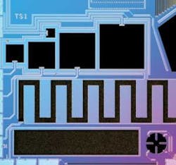
Black silicon is an emerging material in the race to modify silicon for IR detection.5 Black silicon (see Fig. 1) is produced in a complementary metal-oxide-semiconductor (CMOS)-compatible manufacturing process that uses short-pulse lasers to dramatically alter the photoconductive and absorptive properties of silicon. Photodetectors made of black silicon significantly increase the sensitivity of silicon to NIR and SWIR radiation, as well as greatly enhancing response in the bandwidth over which silicon is typically photosensitive. With the IR sensing properties of black silicon, true digital day-night imaging could become as pervasive as visible digital photography is today.
Femtosecond-laser technology is the enabling technology for black silicon. Formed through irradiation with a ultrafast laser in a sulfur hexafluoride atmosphere, the resulting black silicon comprises a highly sulfur-doped, nanostructured surface layer that exhibits room-temperature photoconductive gain and enhanced IR absorption. The manufacturing process is simple, fast, and uses standard silicon fabrication materials and temperatures.
Femtosecond lasers are unique in that they create intense localized conditions in a nearly instantaneous manner without disturbing regions outside the focal volume. For this reason, the industrial use of femtosecond-laser technology has been centered on cutting and drilling applications. However, by using ultrafast lasers in a different context—localized engineering of material form and composition—exciting new opportunities for industrial use of femtosecond lasers are being discovered, such as those presented by black silicon.
Photoconductive gain and absorption
Gain in a photodetector is the phenomenon by which a single photon results in the collection of more than one electron-hole pair by the sensing circuit. “Avalanche” gain and “photoconductive” gain are the most commonly observed gain mechanisms in photodetectors. Whereas avalanche gain (or avalanching) relies on high internal fields and the collisional ionization of atoms within a photodetector, photoconductive gain relies on an asymmetry between the device transit times for electrons and holes in a detector device.6
In comparison to avalanche gain, photoconductive gain operates at low biases and with low noise—characteristics that offer significant advantages for circuit integration, low power operation, and performance. As a result, photoconductive gain is an important attribute of a number of II-VI compound-semiconductor, quantum-well, and cadmium sulfide detectors. In fact, photoconductive gain is one reason cadmium sulfide has the highest room-temperature detectivity (a measure of sensitivity) of any photodetector material.
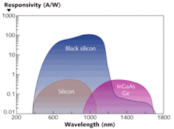
Black silicon enables the first silicon-based photodetectors with efficient, room-temperature photoconductive gain—reaching responsivities of more than 100 A/W in the NIR (see Fig. 2). As such, the amount of signal generated for each photon is comparable to Si avalanche photodiodes, without the added complexity of high voltage and protection circuitry that accompanies avalanche photodiodes. The increased signal from photoconductive gain significantly reduces the burden of signal processing by downstream electronics.In addition to gain, femtosecond-laser processing modifies the absorption properties of silicon. Through a combination of defect engineering and increased optical-path length, black silicon can dramatically reduce the amount of silicon needed to absorb NIR and SWIR light.
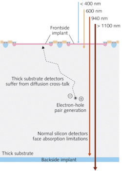
For normal silicon CMOS imagers, the absorption depth of photons in the NIR is so long that most of the light passes through undetected. This is because a CMOS imaging architecture uses less than 10 µm of Si material in the active sensing region. High-performance silicon charge-coupled devices (CCDs) have a very thick sensing region, but remain transparent to wavelengths in the SWIR (greater than 1100 nm), making detection next to impossible (see Fig. 3).The incorporation of black silicon into a detector significantly reduces the absorption depth of NIR and SWIR light so that electron-hole pairs are generated in a thickness of silicon comparable to those used in the CMOS manufacturing process. The combination of increased absorption and high-efficiency photoconductive gain allows the capture and detection of low levels of IR light and opens up a host of new applications to silicon, such as digital night vision, at an affordable cost.
Using black silicon in the NIR and SWIR
Applications for the NIR and SWIR regions are numerous and span the medical, manufacturing, consumer, and defense industries. One of the larger development efforts to use the NIR and SWIR is the pursuit of digital night vision by the defense and security industries. A large amount of ambient light is available over this bandwidth from the natural phenomenon of airglow. Airglow is the emission of light from chemical reactions in the Earth’s atmosphere and contains three prominent spectral peaks between 1000 and 1800 nm. Because silicon cannot perform well enough beyond 1000 nm to be considered an option for digital night vision, typically germanium or InGaAs devices are used in this spectral range. However, these materials are difficult to manufacture in scale, and are noisy and cost-prohibitive for pervasive use on the battlefield or for security cameras.
In contrast, detectors made from black silicon have very high response in the 1000 to 1200 nm range, with responsivity 100 times higher than germanium or InGaAs. Black-silicon devices with sensitivity from 400 to 1550 nm have been produced and work continues with short-pulse-laser material modification to increase sensitivity to wavelengths beyond 1300 nm. The black-silicon laser process opens up a wealth of possibilities for defect engineering through incorporation of activated chemical species to levels difficult to achieve in silicon through more traditional doping methods.
In addition to digital night vision, the region from 1000 to 1200 nm is important in silicon-wafer and solar-cell inspection, plastics sorting for recycling, and noninvasive blood-chemistry monitoring. Specific to the world of lasers, the availability of inexpensive but powerful light sources makes 1064 nm a particularly important NIR wavelength for applications such as free-space communication and laser detection and ranging. However, 1064 nm falls in a region of decreased performance for silicon, germanium, and InGaAs. Silicon rapidly loses sensitivity and has virtually no sensitivity beyond 1050 nm (particularly when cooled) and germanium and InGaAs detectors are at less than 50% of their peak detectivity at 1064 nm. Black-silicon detectors, on the other hand, are near their peak performance at 1064 nm and have higher detectivities than the incumbent commercial technologies.
REFERENCES
- J. L. Tissot et al., Proc. SPIE Infrared Technology and Applic. XXVIII 4820, p. 220 (2002).
- Y. Kang et al., Nature Photonics 3, p. 59 (2008).
- L. Colace et al., IEEE J. Quantum Electronics 43, p. 311 (2007).
- M. W. Geis et al., IEEE Photonics Tech. Lett. 19, p. 152 (2007).
- http://www.sionyx.com.
- Bube, R.H. (1992), Photoelectronic Properties of Semiconductors, University Press, Cambridge.
James E. Carey is a cofounder and Jason W. Sickler is a senior optics engineer at SiOnyx, 100 Cummings Center, Suite 244G, Beverly, MA 01915; www.sionyx.com; e-mail: [email protected].


