Ge-on-Si direct-band-gap LED lays groundwork for group-IV laser
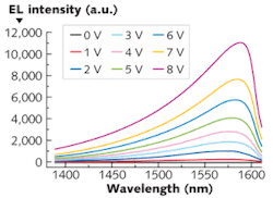
A 1.6-µm-emitting germanium-on-silicon (Ge-on-Si) LED developed by researchers at Stanford University (Palo Alto, CA) could be the key to a Si-compatible group-IV semiconductor laser (useful for optical interconnects and other integrated Si photonics devices). The device, an n+/p homojunction LED, was fabricated using an in situ doping method. Lattice mismatch between Ge and Si provides compressive strain on the Ge, creating a direct band gap; doping with high concentrations of phosphorous and boron shifts the emission wavelength to the relevant 1.6 µm region.
One interesting effect occurring in the new device is that as its temperature increases, so does its output intensity (contrary to what happens in ordinary LEDs). The reason is that at low temperatures, the so-called Fermi-Dirac electron distribution, which determines which electrons contribute to the emission of light, resembles a step function with the step positioned just in the wrong place. At high temperatures, however, the electron distribution gets “smeared out,” with many electrons occupying states that allow them to radiate light. The researchers tested the LED at temperatures ranging from 50 K to 298 K, confirming the effect. Creating a laser would require an even higher doping to achieve gain, say the researchers. Contact Szu-Lin Cheng at [email protected].

