DETECTORS: Near-IR imager uses quantum-dot-sensitized photodiodes
Indium gallium arsenide (InGaAs) photodiodes and quantum-well IR photodetectors are typical methods of choice for near-IR detection and imaging applications in the spectral region around 1 to 2 µm. But because these materials are expensive for large-area devices, researchers have been looking for organic-semiconductor alternatives. Unfortunately, polymers or small-molecule materials with low-enough bandgaps are not efficient as photodetectors in the spectral region above 1 µm. An alternative, however, has been developed by researchers at Siemens Corporate Technology (Erlangen, Germany), the University of Linz (Linz, Austria), and Universität Karlsruhe (Karlsruhe, Germany) that uses solution-processed hybrid diodes from colloidal quantum dots (QDs) and organic semiconductors deposited over a traditional amorphous silicon active-matrix (a-Si AM) backplane to fabricate a flat-panel near-IR imager.1
Quantum-dot sensitivity
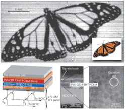
To form the organic/inorganic QD photodiode layer, a mixture of two organic semiconductors, P3HT and PCBM, were combined with lead sulfide (PbS) QDs with diameters ranging from 4.4 to 5.2 nm. Colloidal PbS QDs were chosen due to the effortless scalability of the synthesis and the applicability of the QDs as synthesized for hybrid diodes. With defined diameters for the QDs, the team demonstrated IR diodes with tunable spectral sensitivity up to 1.9 µm. The near-IR photosensitivity is based on the concept of charge separation between an IR sensitizer (being the PbS QDs) and separate electron- or hole-accepting transporting materials (the PCBM and P3HT). An evaporated metal top contact, a polymer interlayer, a bottom electrode, and a 256 × 256-pixel a-Si AM backplane complete the detecting structure (see figure).
To demonstrate operation of the hybrid organic/inorganic photodiode structure, 1310 nm light was passed through a color slide of a monarch butterfly and the cast shadow was imaged. Infrared-image quality is largely dependent on the characteristics of the photodiode layer. Increasing the quantity of QDs in the polymer mixture increases the photoresponse and the dark current of the device; however, 67% by weight of QDs was found to be the optimal percentage for shot-noise-limited performance.
For 4.0 mm2 photodiode devices fabricated separately to test detection performance, spectral sensitivity varied for illumination wavelengths from 870 nm up to about 1450 nm, with external quantum efficiency (EQE) peaking at 51% at 1220 nm. For imaging applications, linear device response as a function of incident light intensity is also important. For these photodiodes biased at -6 V, the photocurrent increases linearly with increasing intensity values from 4.0 µW/cm2 to 0.8 mW/cm2–a constant EQE over more than two decades.
And finally, frequency response was studied in photodiodes fabricated with an active area of 0.8 mm2. For illumination at 1310 nm, the -3 dB frequency was as high as 2.5 KHz, and the -6 dB frequency was 39.5 kHz, suitable for use as a cell-phone imager with a frame rate of 30 Hz. Infrared videos of the imager show low defect density and a pixel-pitch-limited resolution of 154 µm.
Tobias Rauch of Siemens and Ph.D. student at Universität Karlsruhe says, “The actual highlight of our work is the demonstration of diodes with both high rectification and long lifetimes–usually not obtained when using QDs as an infrared absorber.” Project manager Oliver Hayden at Siemens says, “A solution-based diode to achieve highly pixelated near-IR detectors is of high relevance for a number of applications such as night vision. Furthermore, such a scalable technology is of interest for integration on CMOS. But we still need to work on the dark currents, although we have solved this issue already for our organic x-ray detectors.”
REFERENCE
- T. Rauch et al., Nature Photonics 3, p. 332 (June 2009).

Gail Overton | Senior Editor (2004-2020)
Gail has more than 30 years of engineering, marketing, product management, and editorial experience in the photonics and optical communications industry. Before joining the staff at Laser Focus World in 2004, she held many product management and product marketing roles in the fiber-optics industry, most notably at Hughes (El Segundo, CA), GTE Labs (Waltham, MA), Corning (Corning, NY), Photon Kinetics (Beaverton, OR), and Newport Corporation (Irvine, CA). During her marketing career, Gail published articles in WDM Solutions and Sensors magazine and traveled internationally to conduct product and sales training. Gail received her BS degree in physics, with an emphasis in optics, from San Diego State University in San Diego, CA in May 1986.
