BIOSENSING: Photonic-wire biosensor array is sensitive, label-free
A photonic biosensor-array chip created by scientists at the National Research Council Canada (NRC; Ottawa, ON, Canada) contains array sensor elements that can independently and simultaneously monitor different molecular binding reactions.
The monolithically integrated chip, which has spiral silicon photonic-wire waveguides as its elements, is a potential replacement for existing glass microarrays (used in genomics, proteomics, and drug screening) because it has the advantage of sensing molecules directly instead of through fluorescent labels.1 In addition, the arrayed photonic-wire elements have the key capability of providing information such as the strength of the molecular bond, binding-reaction rates, and disassociation rates, says Adam Densmore, one of the NRC researchers.
Conventional glass microarrays are printed with thousands of spots containing different probe molecules, which allow very large numbers of DNA or protein interactions to be studied. The molecules that are being detected are labeled with fluorescent markers that emit light of a specific wavelength when illuminated. After the slide is exposed to the analyte it is washed and then imaged to see if the labeled molecules bound to the individual spots. This method is primarily used to give qualitative yes/no answers—the target molecule is there or is not there. Fluorescent-based detection also requires several extra steps in sample preparation to attach the fluorescent tags; the tags can perturb the binding properties of the system and it is also not always possible to attach tags to certain molecules.
For this reason, says Denmore, surface-plasmon-resonance (SPR) sensors have been commercially developed; these sensors provide more detailed information than fluorescent microarrays, and can monitor molecular binding in real time. However, commercial SPR sensors usually have limited throughput, allowing only one to a few binding reactions to be monitored at a time, although more highly multiplexed systems are beginning to emerge on the market, Denmore notes. SPR sensors are also faced with fundamental limits in terms of their sensitivity.
Array of interferometers
The NRC array provides as much information as SPR sensors, but at a higher sensitivity. In the device, a grid pattern of spiral waveguides was fabricated on a silicon-on-insulator wafer, resulting in waveguides 0.45 µm wide by 0.26 µm thick (the thickness was optimized to provide high sensitivity for the transverse magnetic waveguide mode). Owing to a system of optical splitters and combiners, each spiral waveguide forms the sensing arm of an independent Mach-Zehnder interferometer (MZI).
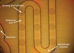
A 2-µm-thick polymer upper cladding was then deposited onto the entire waveguide structure and removed only over the sensing spirals. A second 50-µm-thick polymer layer was deposited and patterned to form a microfluidic channel. Finally, a polydimethylsiloxane (PDMS) cover plate was placed atop the upper cladding (see figure).
Although the PDMS is not glued, surface forces create a good seal, says Denmore. "In addition, our measurement system is designed to draw solutions through our device, as opposed to injecting them, which creates negative pressure within the channel thereby increasing the adhesion," he explains. "The obtained seal is sufficiently strong to prevent fluid or air leakage from occurring during a measurement. After the experiment the cover piece can simply be peeled off of the device, cleaned, and then reused."
Laser light at 1560 nm and TM polarization is delivered to the input of the array. The six output waveguides are simultaneously monitored with an IR camera; the signals nearly saturate the camera, providing a 36 dB dynamic range (12-bit resolution). Phase shifts of the MZIs are determined by fitting the raw intensity data with a cosine function (with phase as a variable).
Real-time measurements were taken of antibody-antigen reactions such as rabbit IgG receptors with antirabbit IgG and other combinations; detection levels of each element corresponded to a surface coverage of less than 0.3 pg/mm2 (the lower the number, the better).
Larger phase shift
"The sensitivity per unit length of our sensor is comparable to that of commercial SPR devices," says Denmore. "The crucial difference between the two is that the surface plasmons used in commercial SPR systems can only propagate about 20 µm before they are absorbed by the gold film. This high propagation loss sets a limit on the sensitivity of these systems. In photonic-wire waveguides, the waveguide mode can propagate over distances of centimeters with little attenuation, thereby producing a much larger phase shift for more accurate measurement."
Denmore expects that the 0.3 pg/mm2 sensitivity can be significantly improved with further engineering of the surrounding measurement hardware. "Also, using our interferometric configuration, we can design our individual sensors to be temperature independent, which reduces the high degree of temperature stabilization required for other sensing schemes," says Denmore. Hundreds of spiral-waveguide elements can potentially be multiplexed together to form high-density sensor arrays.
REFERENCES
- A. Densmore et al., Optics Lett. 34(23) p. 3598 (Dec. 1, 2009).

John Wallace | Senior Technical Editor (1998-2022)
John Wallace was with Laser Focus World for nearly 25 years, retiring in late June 2022. He obtained a bachelor's degree in mechanical engineering and physics at Rutgers University and a master's in optical engineering at the University of Rochester. Before becoming an editor, John worked as an engineer at RCA, Exxon, Eastman Kodak, and GCA Corporation.
