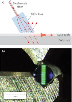
MICRO-OPTICS: GRIN microlens couples fiber output to a planar waveguide

Despite decades of development in optical-fiber and planar waveguides, the pesky problem of how to couple a several-micron-sized optical-fiber beam to a several-hundred-nanometer sized planar waveguide persists. While grating couplers fabricated in photoresist are typically used, they are expensive in small quantities and require complex photolithography methods. And while external focusing lenses and elastomeric, removable gratings have been tried, coupling efficiencies are very low.
One potential solution recently developed by researchers at Laser-Laboratorium Göttingen (LLG; Göttingen, Germany) combines a graded-index (GRIN) lens with a grating structure at its exit face.1 Because this collimating microlens device is removable and reusable, the costs associated with grating couplers (and the waveguide thickness requirements) are eliminated—making the device very appealing as a multiple-use coupler in conjunction with disposable waveguides applied to single-use biosensing applications, for example.
Coupling efficiency
What makes the GRIN coupler superior to conventional micro-optic couplers or tapered-fiber couplers is the fact that its coupling efficiency is comparable to grating couplers fabricated on the surface of planar waveguides. This efficiency is possible thanks to the high-frequency grating structured on the polished surface of the GRIN lens. The structured surface of this lens is then placed in close proximity or in contact with the waveguide (see figure).
The coupling scheme begins with a 0.25 pitch GRIN lens that expands and collimates the light from a singlemode optical fiber. Resonant coupling of the fiber output occurs when the wave vector of the diffracted beam and the wave vector of the guided mode coincide. Using a first-order beam for waveguide coupling, a precise adjustment of the beam angle is achieved by a lateral translation of the fiber exit in the focal plane of the GRIN lens.
To optimize optical parameters of the coupler and quantify coupling efficiency, both software modeling and physical experiments were performed. COMSOL (Burlington, MA) Multiphysics software was used to model the coupling efficiency from the output of a 200 μm wide, 500 nm period sinusoidal structured grating on the endface of the GRIN lens (refractive index n = 1.5) coupled into a 150 nm thick waveguide (n = 2.1) on a 2 μm thick substrate (n = 1.52) with various air-gap widths between the grating and the waveguide surface. For this simulation, the coupling efficiency (the ratio of the power of the port excitation from the coupler to the power that is directed into the waveguide) was greater than 10% for air gaps below 100 nm and as high as 41% with a 20 nm air gap.
Physical experiments were then performed with a 1 mm diameter, 2.58 mm long, 0.25 pitch GRIN lens polished at an angle of 20º with a 500 nm period grating (with a width of 200 μm) structured on its endface using direct laser ablation. Light from a 633 nm helium-neon laser is input to a cleaved singlemode fiber that is then butt-coupled to the GRIN coupler. The TE-polarized light and 0.14 numerical aperture of the fiber produce a collimated beam of approximately 250 μm diameter. The GRIN coupler is then placed directly on the surface of a waveguide chip that consists of a 159 nm thick layer of tantalum oxide (Ta2O5; n = 2.1) over a glass substrate. Maximum coupling efficiency was measured at 13.4% with an air gap of approximately 100 nm.
"This research was fueled by the task to permit reasonably priced disposable waveguides for biosensing applications," says Thomas Fricke-Begemann, project manager at LLG. "However, the coupling scheme can also be used to allow total-internal-reflection microscopy applications on standard microscopes or even on fluorescence readers." He adds, "Of course, we are also open to telecom applications."
REFERENCE
1. T. Fricke-Begemann and J. Ihlemann, Opt. Exp., 18, 19, 19860-19866 (Sept. 13, 2010).

Gail Overton | Senior Editor (2004-2020)
Gail has more than 30 years of engineering, marketing, product management, and editorial experience in the photonics and optical communications industry. Before joining the staff at Laser Focus World in 2004, she held many product management and product marketing roles in the fiber-optics industry, most notably at Hughes (El Segundo, CA), GTE Labs (Waltham, MA), Corning (Corning, NY), Photon Kinetics (Beaverton, OR), and Newport Corporation (Irvine, CA). During her marketing career, Gail published articles in WDM Solutions and Sensors magazine and traveled internationally to conduct product and sales training. Gail received her BS degree in physics, with an emphasis in optics, from San Diego State University in San Diego, CA in May 1986.