CMOS DETECTORS: New techniques recover dynamic range as CMOS pixels shrink
DANIEL VAN BLERKOM, CHRISTOPHE BASSET, and RAMI YASSINE
Anyone who has tried to take an indoor picture with a cell-phone camera of a person standing in front of a brightly lit window has experienced the limited dynamic range of CMOS image sensors. One can either resolve the bright, outdoor scene (in which case the person in front of the window is almost completely black), or the person is well exposed and the outdoor scene is completely saturated and white. When the dynamic range of the scene exceeds the dynamic range of the image sensor, there is severe loss of detail in a portion of the scene and the image quality is generally unsatisfactory.
Extending the dynamic range of CMOS image sensors to create high-dynamic-range (HDR) imagers is of increasing interest in multiple applications. For automotive sensors, where the illumination of a typical scene can vary by many orders of magnitude, HDR operation has become mandatory. It is also of increasing interest as a way to maintain imaging performance with smaller pixels. CMOS image sensor designers are aggressively scaling down pixel sizes to increase resolution and reduce die size. As pixel sizes decrease, however, the intrinsic pixel dynamic range suffers. Fortunately, HDR techniques allow the sensor designer to recover the lost dynamic range and maintain or even enhance imager performance.
Dynamic range
The dynamic range of an image sensor is defined as the maximum output signal of the sensor divided by the noise floor and is reported in decibels (dB). Often these values are referred back to the input and given as equivalent electrons at the pixel photodiode. For example, an image sensor with a "full-well" charge storage capacity of 10,000 electrons with 3 e- (electrons) of input-referred noise would have a dynamic range of 70 dB, assuming no other circuit limits the maximum signal swing in the sensor signal chain.
A dynamic range of 70 dB is fairly typical for consumer CMOS image sensors. Natural scenes can have dynamic ranges greater than 100 dB. Although pixel dynamic range can be increased by making the full-well larger, CMOS processes are moving to lower voltages with smaller-sized pixels, so the trend is in the opposite direction toward smaller full-well pixels.
Reducing noise is also an option, but there is a limit to how low the signal chain noise can be, especially as readout speed increases for video-rate, high-resolution sensors. In addition, for a given supply voltage, increasing the full-well and reducing input-referred noise work against each other. This occurs because the pixel conversion gain, which describes the conversion from electrons in the photodiode to the pixel output voltage swing, decreases for larger full-wells. To refer the noise to the pixel input requires dividing the signal chain voltage noise by the conversion gain; a larger full-well means the input-referred signal chain noise also increases, eliminating any dynamic range improvement.
HDR sensor design approaches
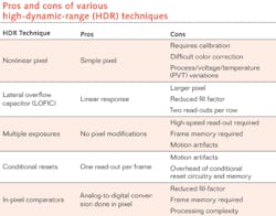
Since the direct approach of increasing the pixel full-well or reducing the noise is limited, several alternatives have been used to create sensors that can capture wide dynamic range scenes (see table). These can be classified into two main groups: techniques that modulate exposure time of the pixels and techniques that modulate conversion gain of the pixel.Nonlinear conversion gain modulation techniques use pixels with a logarithmic response to light, instead of a linear response. A drawback to nonlinear techniques is that they require a lot of calibration and are very sensitive to process, voltage, and temperature (PVT) variations. Another drawback is that the nonlinear output makes proper color correction very difficult across the full range of the sensor output.
Two approaches that maintain linearity are the use of a lateral overflow integration capacitor (LOFIC) in the pixel and the use of two photodiodes (with different sensitivity) in the pixel.1, 2 For these designs, the pixel is read out twice—once for the low-light reading, and again for the high-light reading.
These techniques all require extensive modifications to the traditional pixel design that can lead to degradations in sensitivity and dark-current performance. Modulating the integration time instead of the conversion gain can reduce the pixel modifications required.
The simplest example of this is the use of multiple exposures, which requires no modification to the traditional pixel design.3 The image array is read out multiple times during one frame period, with different integration times. An off-chip frame memory and processing merges the multiple images into the final HDR image. Depending on the number of exposures, the signal chain needs to run significantly faster than in the single-exposure case.
If the pixel integration time can be controlled individually for each pixel, the requirement to read multiple frames can be eliminated. Each pixel output is checked during integration, and a conditional reset is performed depending on how close the pixel is to saturation. A memory is required to store the integration time used for each pixel.
One drawback of the modulated integration time technique is motion artifacts. These occur because integration happens at different times and so captures different portions of the motion across the scene.
Finally, circuitry implementing a comparator can be integrated into the pixel, and the pixel output can be made a digital signal instead of an analog signal. This technique requires significant bandwidth and memory to reconstruct the final image, along with reduced sensitivity due to the additional pixel electronics.Signal to noise
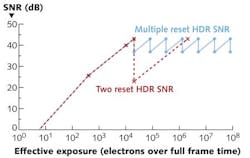
An important feature of these HDR approaches is the potential for the signal-to-noise ratio (SNR) to collapse at the breakpoints between the exposure times or conversion gain changes. For non-HDR sensors at low light levels, the noise floor of the sensor dominates the noise at the output. However, at high light levels, the noise is dominated by the shot-noise of the light being sensed.
When multiple integration time results are merged into a single HDR image, the SNR of the composite image has discontinuities (see Fig. 1). These occur at the switching points between one integration time and the next. If the SNR collapses too much, artifacts can appear in the final image. The minimum SNR that can be tolerated at these points determines the number and ratio of exposures used, and the resulting dynamic range increase.
Tone mapping
Images captured or generated with an HDR sensor are rendered to take advantage of the information contained in the raw image. Commonly available displays, projectors, or printers have a limited contrast ratio that affects the details in the final image. To match the dynamic range of the device, the image is processed through a tone-mapping algorithm that reduces the overall contrast in the image while trying to preserve its details.
Global tone-mapping algorithms such as linear transformation and gamma correction filter the image with the same transformation regardless of the image content. They can result in a washed-out image where details in both the bright and the dark areas are hard to distinguish.
A more content-aware approach can bring out highlights in a scene by locally adapting the image transformation and mapping pixels differently depending on value and that of their nearest neighbors. The simplest way is to isolate details from the image, apply global tone mapping to the image, then re-introduce the unmodified details. Detail extraction is typically done by using a low-pass filter (Gaussian) to blur the image and then subtracting this blurred version from the original image (usually done in the Log domain).4
The key step that most affects tone mapping performance is the extraction of image details and therefore the low-pass filter chosen. Applying a simple Gaussian kernel tends to smooth the sharp contrast areas (such as a dark object in front of a bright background, or vice versa) and creates a halo along the edges. Other methods try to solve this issue at the cost of added computation by using edge-preserving filters that use image content to modify the Gaussian filter kernel for each pixel independently, reducing the appearance of unwanted artifacts.5 These have been popular, with different flavors (bilateral, trilateral) addressing various issues.
The quality of the end result is difficult to quantify; there are no set metrics to measure such a subjective parameter. Contrast can be calculated, but the key performance metric is how natural the scene looks (see Fig. 2). With sensors capable of acquiring images with a greater dynamic range than the human eye, the tone-mapped image may never look right to the observer. The end application dictates what qualifies as a "good" image and what type of metric should be used.
Complex algorithms may work well to post-process captured images but can be challenging to integrate in a compact, autonomous hardware system. Typical hardware implementations use digital signal processors, either as independent chips or as cores in commercially available field-programmable gate arrays (FPGAs) to manipulate floating-point operators and lookup tables needed by tone mapping. Systems integrating the image processing inside the sensor require more streamlined solutions. One approach is to substitute the low-pass Gaussian kernel with a simpler base filter. The image-aware modification can be based on the Euclidian distance of a given pixel to its neighbors. Very wide multipliers are avoided by rounding intermediate products. It yields a more effective circuit in terms of silicon area and power dissipation, at the cost of reduced accuracy and possibly re-introduction of some artifacts. The tradeoff is to balance the hardware resources available and the desired end result.
REFERENCES
- N. Akahane et al., IEEE J. Solid-State Circuits 41, 6, 851–858 (June 2006).
- Y. Wang et al., "A High Dynamic Range CMOS APS Image Sensor," 2001 IEEE Workshop on Charge-Coupled Devices and Ad-vanced Image Sensors (June 2001).
- J. Solhusvik et al., "A 1280 × 960 3.75 µm pixel CMOS imager with Triple Exposure HDR," 2009 Intl. Image Sensor Workshop (June 2009).
- E. Reinhard et al., High Dynamic Range Imaging, San Francisco, Elsevier (2006).
- F. Durand and J. Dorsey, Proc. 29th Conf. on Computer Graphics and Interactive Techniques, 257–266 (2002).
Daniel Van Blerkom is co-founder and CTO, Christophe Basset is a senior scientist, and Rami Yassine is a senior design engineer at Forza Silicon Corp., 2947 Bradley St., Suite 130, Pasadena, CA 91107; e-mail: [email protected]; www.forzasilicon.com.


