PHOTODETECTORS: LWIR plasmonic detector has breakthrough sensitivity and quantum efficiency
Building on earlier work, researchers in the Bio-inspired Sensors and Optoelectronics Laboratory (BISOL) at Northwestern University (Evanston, IL) have developed a long-wavelength infrared (LWIR) photodetector.1
The performance of this quantum-well IR photodetector (QWIP) was enhanced by applying surface plasmons via periodic holes fabricated in a gold-foil layer above the quantum-well structure. For electromagnetic waves normal to the quantum-well surface, a properly designed plasmonic array forms standing waves with a long propagation length, producing a cavity effect that leads to an enhanced transverse plasmonic mode that resonates with electron intersubband transitions in the quantum well and excites additional carriers to generate a strong photocurrent.
Designing the plasmonic array
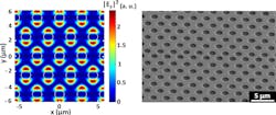
Because photodetection is only enhanced if the wave-generating surface plasmons are perpendicular to the surface (due to the intersubband-polarization selection rule), 3D finite-difference time-domain modeling was used to optimize the surface-plasmon waves and electric-field distribution. By optimizing the surface-normal component of the electric-field intensity distribution at 8 μm (the desired operation wavelength of the LWIR detector), the parameters of the plasmonic array could be determined. Holes with 1.4 µm diameter in a lattice with a 2.9 µm lattice constant were fabricated in a 40 nm thick gold-film layer using focused ion beam (FIB) milling over the semiconductor structure (see figure). This gold layer could also be fabricated over large areas using superlens lithography.2
The quantum-well structure was designed to achieve a peak absorption wavelength of 8 μm with a bound-to-continuum transition. The indium phosphide/indium gallium arsenide (InP/InGaAs) structure includes eight periods of 5.6 nm thick In0.53Ga0.47As doped with a 2.5 × 10¹⁷/cm3 silicon (Si) concentration and 50 nm thick undoped InP quantum barriers. These quantum wells are sandwiched between two highly doped (1018 Si concentration) In0.53Ga0.47As layers 40 nm thick at the top and 500 nm thick at the bottom that form ohmic contacts. The thinner top layer insures maximum proximity of the quantum-well structure to the gold plasmonic layer fabricated on its surface.
Enhanced sensitivity
Analysis of the enhancement ratio of the electromagnetic field for a QWIP structure with and without the plasmonic layer shows that this layer enhances the field by a factor of five. Peak responsivity of the device occurs at approximately 8.06 µm and is as high as 7 A/W for IR light at normal incidence to the detector surface. Because of the strong plasmonic enhancement of the electric field, the measured peak detectivity of approximately 7.4 × 1010 cm Hz1/2/W is a few times higher than for other InP/In0.53Ga0.47As devices operating at a similar wavelength and temperature. In addition, the full-width half-maximum (FWHM) of the absorption spectrum is approximately 0.84 µm, almost half that of identical quantum-well-only structures without the plasmonic layer.
The researchers surmise that this narrow spectral response is due to strong modulation of the QWIP structure by the surface-plasmon resonance of the gold array holes. While a narrow spectrum is favorable to applications that require high spectral resolution, it is less favorable for broadband detection.
Northwestern University associate professor Hooman Mohseni says, "Our plasmonic layer is a perfect match for QWIP, since it addresses the main drawbacks of this technology. Not only does it address the low quantum efficiency of QWIP by enhancing the field intensity, but it also eliminates the natural insensitivity of a QWIP to the normal incident light." Lead author Wei Wu adds, "Interestingly, our plasmonic design also performs as an antireflective coating, and we have plans to create new devices over a broader spectral range."
REFERENCES
- W. Wu et al., Appl. Phys. Lett. 96, 161107 (May 2010).
- W. Wu et al., Nanotech. 18, 485302 (2007).

Gail Overton | Senior Editor (2004-2020)
Gail has more than 30 years of engineering, marketing, product management, and editorial experience in the photonics and optical communications industry. Before joining the staff at Laser Focus World in 2004, she held many product management and product marketing roles in the fiber-optics industry, most notably at Hughes (El Segundo, CA), GTE Labs (Waltham, MA), Corning (Corning, NY), Photon Kinetics (Beaverton, OR), and Newport Corporation (Irvine, CA). During her marketing career, Gail published articles in WDM Solutions and Sensors magazine and traveled internationally to conduct product and sales training. Gail received her BS degree in physics, with an emphasis in optics, from San Diego State University in San Diego, CA in May 1986.
