A single view yields 3D x-ray diffractive images

Aug. 1, 2010
Researchers at the University of California–Los Angeles (Los Angeles, CA), the University of Colorado at Boulder (Boulder, CO), and the University of North Texas (Denton, TX) have for the first time demonstrated ankylography–3D coherent x-ray diffractive imaging that could find applications in imaging thick or embedded structures where slicing for electron or confocal microscopy is not feasible.

Researchers at the University of California–Los Angeles (Los Angeles, CA), the University of Colorado at Boulder (Boulder, CO), and the University of North Texas (Denton, TX) have for the first time demonstrated ankylography3D coherent x-ray diffractive imaging that could find applications in imaging thick or embedded structures where slicing for electron or confocal microscopy is not feasible. From the Greek words "ankylos" and "graphein," ankylography translates to "curved writing" and can produce nanometer-resolution images in 3D from a single, intense femtosecond x-ray pulse from a free-electron laser.

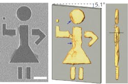
Using a 47 nm tabletop soft x-ray laser spatially filtered to produce a beam with full spatial and temporal coherence, the research team focused the beam using two multilayer mirrors onto a test sample. The researchers then measured the x-ray diffraction pattern on a large-area x-ray CCD a mere 1.7 cm away. Because the high-numerical-aperture diffraction pattern recorded on a flat CCD detector is distorted, mapping this flat pattern onto a curved Ewald sphere reveals 3D information for the object since the sphere is a hemispherical slice through the 3D reciprocal space of the test object. Using a phase-retrieval algorithm, a 3D rendering of a 7 µm tall stick figure cut from 100 nm thick gold on 100 nm thick silicon nitride was recovered; however, the technique requires accuracy improvements before it can be practically applied. Contact Jianwei Miao at [email protected].
Sponsored Recommendations

Brain Computer Interface (BCI) electrode manufacturing

Jan. 31, 2025
Learn how an industry-leading Brain Computer Interface Electrode (BCI) manufacturer used precision laser micromachining to produce high-density neural microelectrode arrays.

Electro-Optic Sensor and System Performance Verification with Motion Systems

Jan. 31, 2025
To learn how to use motion control equipment for electro-optic sensor testing, click here to read our whitepaper!

How nanopositioning helped achieve fusion ignition

Jan. 31, 2025
In December 2022, the Lawrence Livermore National Laboratory's National Ignition Facility (NIF) achieved fusion ignition. Learn how Aerotech nanopositioning contributed to this...

Nanometer Scale Industrial Automation for Optical Device Manufacturing

Jan. 31, 2025
In optical device manufacturing, choosing automation technologies at the R&D level that are also suitable for production environments is critical to bringing new devices to market...

Voice your opinion!

To join the conversation, and become an exclusive member of Laser Focus World, create an account today!