PHOTONIC FRONTIERS: SILICON PHOTONICS: Nonlinear optical techniques raise silicon photonics promise

Will nonlinear optics be the sparkplug for success of silicon photonics? Experiments in recent years have shown that silicon (Si) nanowires have strong nonlinearities that can be powerful tools for manipulating light. Produced using standard Si fabrication technology, Si nanowires could be integrated with other Si components for on-chip signal processing, or serve as nanoscale components of other systems.
Nonlinear optics was born half a century ago, when the ruby laser for the first time concentrated coherent light to the high intensities needed to produce nonlinear effects that have since found applications ranging from green laser pointers to femtosecond frequency combs. Silicon photonics likewise can concentrate light to high intensities, in Si waveguides or "nanowires" with submicrometer cross-sections, which by tightly confining light in a very small area can produce nonlinear effects at modest powers. That could lead to compact nonlinear devices for use on chips.
Fundamentals of Si nanowires
Crystalline silicon has a centrosymmetric structure, so it lacks second-order nonlinearity, but it has a very large third-order nonlinear susceptibility–a factor of 1000 to 10,000 larger than that of silica. Its nonlinear properties in nanowires also depend on the strain applied to the material and how the structure confines light.
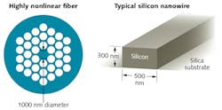
Fabricating the nanowire such that it creates strain induces a second-order nonlinearity within the silicon, so it can produce effects not present in the bulk material. How tightly a waveguide can confine light depends on the refractive index contrast between the core of the waveguide and the cladding. For Si, with refractive index of 3.5, the confinement is very strong when clad with silicon dioxide (n = 1.45) or in direct contact with air. This allows light guiding in nanowires with cross-sections of less than 0.1 mm2. Typical rectangular waveguides are deposited on silica, with width of 375 to 800 nm, and thickness of 225 to 400 nm. Figure 1 compares the structure of a nanowire with that of a highly nonlinear optical fiber.
Thanks to the tight confinement, the optical field density is high in these tiny Si waveguides. The structure also allows dispersion engineering and its geometry allows carriers to diffuse rapidly to the surface. These factors combine to produce a strong nonlinearity so that only a few hundred milliwatts can produce significant third-order nonlinear effects in nanowires of a few hundred micrometers to a few millimeters long.
Dispersion depends strongly on waveguide geometry, so careful selection of dimensions can tailor properties such as group-velocity dispersion, phase index, pulse compression, phase-matching, and soliton generation. Thus it's possible to select geometry to produce a particular zero-dispersion wavelength or to produce anomalous dispersion at specific wavelengths required for some applications.
Nonlinear effects demonstrated
It doesn't take much power to drive Si nanowires into a strongly nonlinear regime. Peak pump powers of 1 W can generate intensities of a gigawatt per square centimeter inside a 220 × 450 nm waveguide, "sufficient to readily observe all of the key nonlinear phenomena in optical fiber," writes Richard Osgood of Columbia University (New York, NY) in an excellent review paper.1
Demonstrations of Raman scattering and gain in Si waveguides date back to experiments in the early 2000s by Ricardo Claps and colleagues at the University of California at Los Angeles, but realizing the high potential Raman gain requires overcoming problems.2, 3 One is that two-photon absorption generates current carriers that absorb light in the waveguide. Carrier concentration can be controlled by pulsed excitation or by applying a bias across the waveguide to extract them.
Two-photon absorption is the main factor that optically limits femtosecond pulses–it can limit peak output powers to about 50 mW, with saturation at higher powers. Other nonlinear effects limit output with longer pulses.
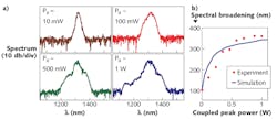
As in optical fibers, self-phase modulation spreads the frequency of input laser pulses in a nanowire, with the spreading increasing with pump power. Two-photon absorption and the carriers it produces can strongly affect self-phase modulation. At pulse lengths below one picosecond, third-order dispersion also can contribute to the spectral modulation, and by the time pulse length reaches 200 fs, free-carrier absorption has become weak and third-order dispersion dominates, making the spectrum asymmetric (see Fig. 2).Cross-phase modulation can occur when two or more pulses pass through a nanowire. However, the effects are different from those in fiber because they are influenced by two-photon absorption and strong dispersion in the nanowire. Experiments have demonstrated wavelength shifts of more than 10 nm, which could lead to applications in optical switching.
Solitons can be generated at wavelengths where a waveguide material has anomalous dispersion. The effective nonlinear coefficient of Si nanowires is so much larger than that of silica that soliton effects can be produced in nanowires just millimeters long.
Four-wave mixing and some other parametric processes have also been demonstrated in Si nanowires. These third-order processes require a strong Kerr nonlinearity and phase matching, which can be achieved by control of waveguide dispersion, as mentioned earlier.
Applications
These demonstrated capabilities open prospects for a range of Si nanowire applications based on manipulating light in various ways.
Nonlinear spectral broadening was first demonstrated in the 1960s and has been extended to supercontinuum generation in highly nonlinear optical fibers. However, lengths of several meters are required even for the most nonlinear silica fibers, photonic crystal fibers with effective mode areas of about 1 μm2. Silicon nanowires can achieve similar results in much shorter lengths. For example, a 2007 experiment broadened 1.3 μm pulses by more than 350 nm in a 4.7 mm Si nanowire (see Fig. 3).4 Yet challenges remain in engineering the system to avoid limitations such as two-photon absorption, and strong broadening is thought to require anomalous dispersion at the pump wavelength.Pulse compression is another potential application. One approach is to use dispersion engineering analogous to dispersion management in fiber systems. Another is to use cross-phase modulation, with a strong pump beam shifting the phase of the signal beam at a wavelength with anomalous dispersion.
Many potential applications involve high-capacity data communications or processing on or between chips. Four-wave mixing might be used to regenerate weak or noisy input signals, which requires reshaping the pulses, reducing the error ratio, and reducing the timing jitter. A 2008 experiment reported all three types of regeneration, including reduction of root-mean-square jitter by a factor of 2.2 in a 1 Gbit/s return-to-zero (RZ) data stream.5 Another experiment showed that stimulated Raman scattering in a nanowire could delay signals by an amount proportional to the intensity.6
A particularly intriguing demonstration last year showed that cross-phase modulation in a Si nanowire could convert signals from one standard telecommunications format to another. The input was a 10 Gbit/s non-return-to-zero (NRZ) signal with on-off keying, which was passed through a purely passive 5 mm nanowire and detuned filter to generate an RZ code with the same on-off keying and polarity preserved.7 That's an important practical problem, because less expensive NRZ equipment is widely used for relatively short transmission distances in metropolitan networks, but more costly RZ equipment is used to meet higher performance requirements in long-haul networks.
Outlook
Nonlinear silicon photonics is in the exciting stage of exploring the frontiers of a new technology. Developers have the advantage of starting from our well-established understanding of bulk nonlinear optics, fiber-optics, and photonic crystal concepts, but they also must overcome challenges posed by the limitations of Si waveguides.
One of those challenges is the two-photon absorption in Si, which affects wavelengths at which the photon energy is more than half of the bandgap energy in Si. It affects the 1550 nm telecommunications band and limits parametric gain to several decibels. Osgood's group recently showed that shifting to 2200 nm, where photon energy is just below half the bandgap energy, slashed two-photon absorption. The group measured broadband gain as high as 25.4 dB from a 4 mm chip, which compensated for all insertion losses and left a net gain of 13 dB.8
Shifting to 2200 nm poses its own challenges, particularly the need for good laser sources. However, Sanja Zlatanovic and Jung S. Park of the University of California at San Diego (La Jolla, CA) showed that two-stage mixing of telecommunications-band sources, with the final stage in a Si waveguide, could generate light tunable near 2388 nm.9 Like most research in the field, it has a way to go, but signs are encouraging.
REFERENCES
1. R.M. Osgood et al., "Engineering nonlinearities in nanoscale optical systems: physics and applications in dispersion-engineered silicon nanophotonic wires," Adv. in Opt. and Photon., 1, 162-235 (2009).
2. R. Claps, D. Dimitropoulos, Y. Han, B. Jalali, "Observation of Raman emission in silicon waveguides at 1.54 μm," Opt. Exp., 10, 1305-1313 (2002).
3. R. Claps, D. Dimitropoulos, V. Raghunathan, Y. Han, and B. Jalali, "Observation of stimulated Raman amplification in silicon waveguides," Opt. Exp., 11, 1731-1739 (2003).
4. I.-W. Hsieh et al., "Supercontinuum generation in silicon photonic wires," Opt. Exp., 15, 15242-15249 (2007).
5. R. Salem, M.A. Foster, A.C. Turner, D.F. Geraghty, M. Lipson, and A.L. Gaeta, "Signal regeneration using low-power four-wave mixing on silicon chip," Nat. Photon., 2, 35-38 (2008).
6. Y. Okawachi, M. Foster, J. Sharping, A. Gaeta, Q. Xu, and M. Lipson, "All-optical slow-light on a photonic chip," Opt. Exp., 14, 2317-2322 (2006).
7. W. Astar et al., "Conversion of 10 Gb/s NRZ-OOK to RZ-OOK utilizing XPM in a Si nanowire," Opt. Exp., 17, 12987-12999 (July 20, 2009).
8. X. Liu et al, "Mid-infrared optical parametric amplifier using silicon nanophotonic waveguides," Nat. Photon., DOI: 10.1038/ NPHOTON.2010.119.
9. S. Zlatanovic et al., "Mid-infrared wavelength conversion in silicon waveguides using ultracompact telecom-band-derived pump source," Nat. Photon., DOI: 10.1038/ NPHOTON.2010.117.

Jeff Hecht | Contributing Editor
Jeff Hecht is a regular contributing editor to Laser Focus World and has been covering the laser industry for 35 years. A prolific book author, Jeff's published works include “Understanding Fiber Optics,” “Understanding Lasers,” “The Laser Guidebook,” and “Beam Weapons: The Next Arms Race.” He also has written books on the histories of lasers and fiber optics, including “City of Light: The Story of Fiber Optics,” and “Beam: The Race to Make the Laser.” Find out more at jeffhecht.com.

