QUANTUM-DOT DETECTORS: Colloidal quantum-dot phototransistor could become solar-cell junction
The concept of using a phototransistor to capture light instead of a photodiode or a photoconductor is an attractive one. A phototransistor—for example, a photo field-effect transistor (photoFET)—can potentially provide the gain of a photoconductive detector but with a lower dark current.
To create a practical photoFET, four things must happen. First, photoelectrons must be transferred from the sensitizing material to the electron-accepting channel (EAC). Second, recirculation of secondary injected photocarriers flowing along the EAC should cause a photocurrent. Third, a sensitizing layer thick enough to absorb all the light should efficiently inject all carriers into the EAC. And finally, the EAC must be made thin enough to produce a low dark current.
Progress is being made toward a usable device: Researchers at the University of Toronto (Toronto, ON, Canada) have reported achieving the first two out of these four goals by creating a tunable quantum-dot photoFET based on lead sulfide (PbS) colloidal quantum dots (CQDs) as the sensitizing material.1 The photoFET has a bandgap that is tunable by modifying the properties of the CQDs.
Tests with differing bandgaps
The CQDs are deposited in the form of a “submonolayer,” or a patchwork distribution of unconnected monolayer quantum-dot areas intermingled with areas free of CQDs. Because the CQD patches do not touch each other, the arrangement does not enhance the conductivity of the layer; this is intentional, as the researchers’ experiment is meant to concentrate on electron injection into the channel rather than conductivity-enhancing treatments.
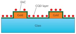
The EAC was made of 50-nm-thick aluminum-doped zinc oxide (AZO), which was deposited on a glass substrate on top of prepatterned gold electrodes (see Fig. 1). For study purposes, the spaces between the 3-mm-long electrodes ranged between 2.5 and 100 μm. Three different types of AZO film were deposited on separate devices under oxygen partial pressures of 5%, 10%, and 20% (the higher the oxygen partial pressure during deposition, the higher the electron affinity and the lower the conductivity of the AZO film). The CQDs, which were dispersed in octane at a density of 0.5 mg/mL, were spun-cast onto the AZO, with the AZO near the contact pads removed so that the submonolayer covers only areas that are active. Using scanning-electron microscopy, the researchers checked to make sure that the CQD films were discontinuous.
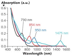
Different batches of CQDs were created with differing quantum-dot sizes, producing bandgaps of 730, 854, 950, and 1475 nm (see Fig. 2). Otherwise identical devices were fabricated with these four different bandgaps. All samples were tested under the same conditions: 627 nm light incident at an intensity of 225 μW/cm2 and modulated at 0.2 Hz. The device was subjected to a voltage of 1000 V/cm for all measurements.The photoconductive gain increased as the size of the CQDs increased; this was attributed to the higher absorption of the red light for the larger quantum dots. However, for all CQD sizes, the photoelectron transfer was efficient. For CQDs that produced a 727 nm bandgap, the output current varied between 4.1 to 6.2 nA during modulation for 5% oxygen-rich AZO channels, and between 2.05 and 2.25 nA for 20% oxygen-rich channels. For a 1475 nm bandgap, the output varied between 113 and 122 nA during modulation for 5% oxygen-rich channels, and between 23 and 27 nA for 20% oxygen-rich channels.
As the oxygen enrichment in the AZO film was increased, the temporal response of the device improved and the dark current decreased; this is due to the lower trap density at higher oxygen-vacancy levels. The temporal response also improved for larger quantum dots (longer-wavelength bandgaps). These effects allow the properties of the photoFET to be optimized for a particular wavelength range by optimizing QCD size and AZO film fabrication conditions.
A separate experiment in which the illumination intensity was varied revealed that the external gain decreased at higher intensities; this effect was consistent for all CQD bandgaps and AZO film types.
For comparison, the researchers decided to test their configuration using sputtered titanium dioxide (TiO2) as the electron-accepting channel material; TiO2 works well when used in CQD solar cells, and has a band-edge position that is similar to that for AZO as well. The TiO2-based devices had a quicker temporal response but an external gain at least ten times lower than that for the AZO-based photoFETs.
Potential infrared photovoltaic junction
One application for which the CQD photoFET could be especially well suited is photovoltaics. Multijunction solar cells have especially high efficiency because they contain anywhere from two to four layered junctions, each optimized for a different wavelength band. Such solar cells can be designed to function across the visible spectrum, or work for a combination of visible and infrared. Because the external gain of the AZO-based photoFET is higher at longer wavelengths, the University of Toronto researchers believe that it could someday be used in a high-efficiency triple-junction solar cell designed for longer wavelengths as the smallest-bandgap junction, which would require a bandgap of about 1600 nm.
First, though, the electron mobility of the CQD sensitizing layer in the AZO-based device must be raised so that a layer thick enough to absorb all photons will shuttle a high proportion of the dissociated electrons into the EAC.
REFERENCE
1. S. Ghosh et al., Appl. Phys. Lett., 99, 101102 (2011).

John Wallace | Senior Technical Editor (1998-2022)
John Wallace was with Laser Focus World for nearly 25 years, retiring in late June 2022. He obtained a bachelor's degree in mechanical engineering and physics at Rutgers University and a master's in optical engineering at the University of Rochester. Before becoming an editor, John worked as an engineer at RCA, Exxon, Eastman Kodak, and GCA Corporation.

