PHOTONICS APPLIED: MATERIALS PROCESSING: Microwelding demands new laser tools
The growing medical device industry, a rapid increase in automotive sensor sales, and the rebound of the telecommunications industry have driven a need for joining conductive materials such as copper, silver, and gold. Welding these materials is problematic for any technology and has even proved extremely difficult or impossible with traditional 1064 nm pulsed neodymium:yttrium aluminum garnet (Nd:YAG) laser-welding technology. But a recent innovation—a frequency-doubled 532 nm green Nd:YAG pulsed laser capable of 4 J pulse energies—offers nearly an order-of-magnitude increase in material absorption over the 1064 nm wavelength, expanding and legitimizing the use of lasers in conductive microwelding applications.
Microwelding drivers
As part miniaturization continues and connector sizes decrease below 0.004 in. thicknesses for flat ribbons and wire diameters, such traditional processes as crimping, soldering, and brazing become less viable due to high joint resistance and questionable joint reliability and longevity. By contrast, welding, which provides excellent joint integrity, longevity, and conduction performance, is quickly becoming the required standard. For joining two materials where at least one is <0.02 in. thick, the process is called “microwelding.”
Copper is typically the material of choice for electrical connections due to its superior ability to efficiently conduct electrical energy and transmit signals. In addition, silver and gold are used either as plating materials or for the conductor itself. However, the very high thermal conductivity that makes copper, gold, and silver such good choices as conductors rapidly pulls heat away from the weld joint, making it difficult to maintain heat balance and weld reliability. This difficulty is further exacerbated by trends toward increased production rates, reduced part size, and welding of dissimilar materials and dissimilar conductor cross-sections.
The challenge of microwelding these materials is how to control the heat balance in these small and highly conductive parts to enable welding while ensuring no over- or under-heating. One way of meeting this significant challenge is by using a 532 nm green laser.
Traditional microwelding
Traditional microwelding technologies such as ultrasonic bonding, resistance welding, and laser welding have their own advantages and disadvantages. Ultrasonic welding is particularly well suited to sheet and foils welding of conductive parts, including aluminum and copper.
However, the ultrasonic process has some drawbacks: Since force is imparted onto the parts, mechanical contact is required on either side of the joint. In addition, the horn is a consumable that requires inspection and replacement. Joint geometry is somewhat limited to lap welding only and accessibility of the horn design. Finally, plated materials are sometimes problematic and the speed of the welding cycle that involves actuation of the horn can slow production rates.
Resistance welding uses the weld interface’s high resistance to create heat as current is passed through the parts. The circuit is created by electrodes that contact the part either from the same side or opposite sides of the workpieces. Electrical contact is ensured by exerting some force on the parts.
While resistance welding works well for a wide variety of joining applications and materials, it relies on mechanical contact and the need to create an electrical circuit between two electrodes. It may not work properly in all circumstances, especially if the parts are mechanically delicate and themselves highly conductive. In addition, the minimum electrode size is around 0.04 in. in diameter, limiting joint accessibility.
Laser welding is a noncontact process, requiring only single-sided access. The technology is useful for working on extremely small joint areas, and can be used to weld different-shaped parts, different joint geometries, and dissimilar materials. It uses no consumables that need to be maintained or replaced and the weld cycle is measured in milliseconds.
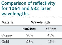
On the face of it, laser welding appears to be an excellent solution for copper microwelding—but there is a problem. The pulsed Nd:YAG lasers used for the majority of materials processing applications have a wavelength of 1064 nm, which is more than 90% reflected by copper. Extremely high power is required to overcome the reflectivity and ensure that sufficient light energy is delivered to the copper to initiate the weld. However, once enough laser power is delivered to the copper to raise its temperature, the reflectivity decreases.
Because the absorption occurs in time scales of less than a millionth of a second, there is a rapid change in how much power is absorbed; that is, the high power that was initially required now far exceeds what is required to form the weld. As a result, the material rapidly overheats and vaporizes, leaving a large porosity or a hole.
A number of techniques have been used in an attempt to overcome this reflectivity, including pulse shaping, oxygen assist, and the use of less reflective platings. However, few have been successfully used in production due to practical implementation and process reliability concerns.Pulsed green lasers
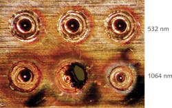
Reducing the laser wavelength from 1064 nm to 532 nm significantly reduces the reflectivity of copper and other conductive materials (see table). The 532 nm (green) wavelength enables consistent coupling into the copper and stabilizes welding (see Fig. 1).
Using the process of second harmonic generation (SHG), 532 nm laser light can be produced from a 1064 nm lamp-pumped solid-state (LPSS) laser. The SHG process uses a frequency-doubling crystal that operates as a nonlinear optic.
Simply put, the incident laser frequency induces an electric field within the crystal that is out of sync with the incident field. The crystal then re-radiates at a different frequency and therefore a different wavelength to the laser that initiated the effect. The frequency-doubling crystal—either lithium triborate (LBO) or potassium titanyl phosphate (KTP)—can be located either inside or outside the laser cavity.
Traditionally, 532 nm lasers have been used for marking or micromachining applications. The high peak power of Q-switched lasers offers efficient conversion in the crystal, where typically a 50% loss in power is standard. Therefore, 10 W in provides 5 W out. However, these Q-switched lasers have a pulsewidth of 50–100 ns and pulse energies typically <1 mJ. This is adequate for marking and micromachining, but way below what is needed for welding, where even the smallest microweld requires 100 mJ up to 1 J.
Miyachi Unitek’s 532 nm laser welder is capable of up to 4 J pulses, which covers the majority of microwelding applications. The challenge for our SHG welding laser was to achieve efficient conversion with two orders-of-magnitude lower peak power. Such a laser was developed by placing the crystal within the cavity and with careful control of polarization and beam power density on the crystal.
In the final version, the 532 nm pulsed Nd:YAG welding laser is capable of 1.5 kW peak power with up to 5 ms pulsewidth. This provides enough weld energy to penetrate approximately 350 µm thick oxygen-free copper, which is sufficient for many micro-conductor welding applications. All the benefits of a regular pulsed YAG laser are maintained, including real-time power feedback, flat-top modes, fiber delivery, and time and energy shared outputs.
Microwelding examples
Electrical connections come in many different sizes, shapes, and materials. The requirement for high-quality, reliable terminal connections occurs in many industries, and the welding of electrical contacts needs to create a conduction path that is seamless to the operation of the part such that the joint performs as a single, solid, continuous component. Laser welding offers this potential.
For example, the automotive industry has seen a significant increase in sensor technology to monitor car performance, functionality, and environment. Each sensor has many terminal connections that must survive for the lifetime of the car. In this arena, laser microwelding provides a viable option.
Connection requirements are also important in the medical industry in implantable devices and sensing/monitoring instruments, where each connection is essential to maintaining part functionality and performance. Similarly, in the communications industry, signal strength and integrity are crucial to maximize part performance and ensuring that the joint is not a limiting factor in the part’s design.
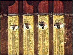
A common connection in the electronics industry is bonding 0.0015-in-thick gold-coated copper flat wire to metallized pads. Ideally the pad thickness is at least 1.5 times the thickness of the ribbon, creating a good thermal balance between the wire and the pad and preventing the pad from overheating.For high-volume production, welding multiple joints on lead frames is all about quality and speed. Being a noncontact process, laser welding lends itself to volume manufacturing by executing many welds per second depending on the effectiveness of motion integration with the weld tool (see Fig. 3). By removing the barrier of high reflectivity for 1064 nm laser microwelding of conductive metals, the 532 nm green Nd:YAG laser welder offers a viable method for microwelding copper and other conductive materials in high volume.
Geoff Shannon, Ph.D. | Director Strategic Marketing for Precision Manufacturing, Coherent
Geoff Shannon, Ph.D., is Director Strategic Marketing for Precision Manufacturing at Coherent (Santa Clara, CA) and an Editorial Advisor to Industrial Laser Solutions. He previously served as Laser Technology Manager for Miyachi Unitek, specializing in the development of lasers and applications for existing and new markets. Shannon has a BEng in Mechanical Engineering and PhD in Laser Welding Technology from the University of Liverpool. His 20-year career in laser technology has centered around applications research and development and new product development of lasers and systems.


