PHOTONIC FRONTIERS: NOVEL LASERS: The incredible shrinking laser makes a big impact

We often think of lasers as macroscopic devices, with resonant cavities thousands of wavelengths long and emitting areas large enough to generate thin diffraction-limited beams. Yet semiconductor lasers the size of grains of salt have been around for decades, and even smaller microlasers have been demonstrated in the lab.
Now the cutting edge has moved to nanolasers, with dimensions on the order of—or even smaller than—a single wavelength. Reaching that scale requires fundamentally new laser designs, and recent years have seen significant progress. Laboratory demonstrations have moved from optical pumping at cryogenic temperatures to room-temperature operation. Much remains to be done, but developers envision potential applications in areas including sensing and on-chip communications.
Seeking subwavelength lasers
Semiconductor lasers are leading the race to smaller sizes. Innovations such as whispering-gallery ring microresonators and photonic-crystal cavities shrank them markedly, but those technologies have their own limitations. Whispering-gallery resonators must have diameters significantly larger than a wavelength. Photonic-crystal resonators require many cycles of a photonic-crystal material to achieve adequate reflection and cavity quality factor, making them multiple wavelengths long.
Most of the new generation of nanolasers produces light energy within a semiconductor, but the details differ greatly. The first to be demonstrated was a semiconductor “nanowire,” typically 10 to 100 nm in diameter and 1 to 100 µm long. More recently, metal-clad semiconductor nanolasers have been developed, in which the metal cladding confines light inside a wavelength-scale or smaller semiconductor structure. The two have quite different structures and characteristics.
Achieving laser emission from subwavelength devices requires structures that include metal elements. A purely dielectric laser can have a cavity no smaller than half a wavelength on each side, says Shun Lien Chuang of the University of Illinois at Urbana-Champaign (Urbana, IL). Emission from smaller structures requires producing surface plasmons, groups of electrons at the boundary between a metal and a semiconductor or dielectric, which oscillate at optical frequencies and thus radiate light. The challenge is how to overcome metal optical (absorption) loss. The devices can be considered as optical-frequency counterparts of subwavelength radio antennas.
Nanowires
Nanowires are semiconductor filaments, typically fabricated by depositing a high-bandgap semiconductor. Confinement of light within nanowires is much higher than in conventional semiconductor waveguides because the high-index semiconductor is exposed to air, making them attractive laser candidates. So far, laser emission has been demonstrated from a variety of semiconductors, mostly with high bandgaps emitting at visible or ultraviolet wavelengths. Virtually all nanowire lasers have been optically pumped.
At first glance, nanowire lasers seem to have Fabry-Perot cavities because they have reflective surfaces at both ends, but it’s not that simple. The actual behavior of the reflective surfaces is much more complex because they are comparable to or smaller than the wavelength, Cun-Zheng Ning of Arizona State University (Tempe, AZ) wrote in a review paper published last year.1 The small size and strong waveguide effect also makes emission strongly divergent in the far field.
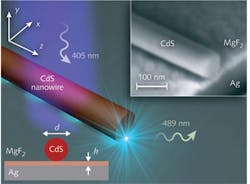
Fabrication of a semiconductor nanowire on a metal substrate opens other possibilities arising from the interaction of the optical-frequency field in the nanowire with surface plasmons at the metal-semiconductor interface. Xiang Zhang’s group at the University of California–Berkeley (Berkeley, CA) demonstrated a plasmonic laser by optically pumping 50-to-100-nm-thick cadmium-sulfide nanowires with 405 nm light. Interaction of light produced in the CdS with the silver on which the nanowire rested produced surface plasmons, which emitted 489 nm light in a 10 nm strip where the two materials were in contact, as shown in Fig. 1.2 The surface plasmons propagated parallel to the wire.
That was an important demonstration because it showed how narrow an area could be made to emit light—the strip was only 1/25 of a wavelength wide, far beyond traditional optical limits. However, like most nanowire lasers, it was optically pumped, which is considered undesirable for many potential applications—such as on-chip communications—because it requires an external laser source.
A different surface plasmon configuration was used in the smallest laser yet demonstrated, called a “spaser” for surface-plasmon amplification by stimulated emission of radiation. Mikhail Noginov of Norfolk State University (Norfolk, VA) and colleagues optically pumped 14 nm gold spheres coated with a 15 nm layer of silica in which dye molecules were embedded. Pumping with 480 nm light produced stimulated emission at 531 nm from surface plasmons interacting with dye molecules. The spaser emitted light across its entire surface.3Metal-clad semiconductor nanolaser
Metal-clad semiconductor nanolasers mark “a paradigm shift in laser design,” Ning told CLEO in May 2011. Martin Hill first demonstrated one four years ago at the Technical University of Eindhoven (Eindhoven, the Netherlands), and the design has gained favor since.4
One key advantage of coating a semiconductor light emitter with a metal is that a metallic cavity can better confine light, Shun Lien Chuang of the University of Illinois at Urbana-Champaign (Urbana, IL) said at CLEO 2011. Electromagnetic fields tend to leak out of small volumes of dielectric materials, but the metal coating provides much better confinement and can isolate nearby devices to prevent crosstalk. Another advantage is that the structure lends itself to electrical pumping.
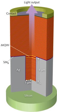
Chuang’s group, in collaboration with Dieter Bimbert’s group at the Technical University of Berlin, has concentrated on nanolasers slightly larger than a wavelength. The cylindrical semiconductor core of their structure, shown in Fig. 2, resembles a vertical-cavity surface-emitting laser (VCSEL), with its gallium-arsenide substrate etched away; it was coated with silver and flip-chip bonded to a silicon substrate.
They reported continuous-wave room-temperature operation of electrically pumped devices with multiple quantum wells in their active layers. A distributed-Bragg reflector stack and a metal layer formed the cavity. The structure includes an insulating silicon-nitride layer to isolate terminals of the diode. They have reported output of more than 8 µW in a 995 nm emitter with threshold current about 2.6 mA.5 They also have demonstrated other versions.
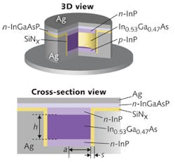
“Our laser preserves the advantages of circular beam shape of VCSELs, [offering] efficient coupling to fiber or free-space optics. The complete metal encapsulation, the removal of the GaAs substrate, and metallic bonding to silicon ease the serious heat accumulation in conventional semiconductor lasers. It is our belief that our approach and structure make room-temperature operation of nanolasers with significant output power promising for the near future,” says Chuang.Chien-Yao Lu and Chuang have also proposed smaller “nano-coin” lasers, shown in Fig. 3 which would reduce the large metallic losses that so far have limited nanolaser performance.6 Instead of having a DBR stack, the top and bottom metal layers would serve as reflectors. They say nanolasers smaller than 0.01 cubic wavelength could have reasonable gain. At CLEO 2011, Akira Matsudaira of Illinois reported LED versions about 2 µm in diameter and 200 nm thick, emitting at 1550 nm. The encapsulated volume was only 0.76 cubic micrometer, corresponding to 0.19 cubic wavelength in vacuum.7
Subwavelength hybrid lasers
Ning’s group at Arizona has gone further with subwavelength metal-coated semiconductor nanolasers. At CLEO 2011, Ning reported the first continuous-wave, room-temperature operation of subwavelength lasers, with volumes of 0.92 and 0.4 cubic wavelength.
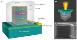
In 2009, Hill and Ning collaborated to make a laser in which one dimension of the cavity was reduced to less than half a wavelength.8 They etched rectangular pillars as thin as 90 nm, and tested laser operation in cavities a few micrometers long. They recorded laser action in the 1500 nm range at cryogenic temperatures in the 90 nm pillars coated with 20 nm of metal—the thinnest laser on record—and demonstrated pulsed room-temperature operation in a 310-nm-thick pillar.Since then, Ning’s group has been working with Hill on shrinking their lasers in the two other dimensions, adapting the etched design. At CLEO, Ning described progress on metal-semiconductor nanolasers of the design shown in Fig. 4. Two of his earlier subwavelength lasers had already operated continuous-wave at 260 K. One measured 1.1 × 2.15 × 1.55 µm, equivalent to 0.96 wavelength at its 1563 nm output. A longer, thinner device, measuring 280 nm × 6 µm × 1.53 µm (0.78 cubic wavelength at its 1489 nm output) oscillated on multiple modes of the Fabry-Perot cavity.9
Beam quality suffers because the emitting area is small, but that is not a major drawback, Ning says. “These lasers are mostly intended for very close applications on chips,” where they might sit directly on silicon waveguide for optoelectronic integration. Small size is crucial for those applications. “If optical devices are a thousand times larger than transistors, that’s a mismatch. Our dream is to shrink optical devices down to the order of the size of the electronics,” says Ning.
How small can lasers go?
It’s only natural to ask how small lasers can go. In theory, it looks possible to make metal-clad 20 nm cubes with a 10 nm semiconductor core, which have a distinct laser threshold, says Ning. “The only problem is that it’s become a point source” at that size. It would radiate in all directions, with no directional beam.
Such a tiny device could help solve the tough problem of transmitting signals around tomorrow’s high-performance electronic chips. But it also raises a big question: What is a laser? In a world where a living cell can be called a laser, that’s a very interesting problem.
REFERENCES
1. C.-Z. Ning, “Semiconductor nanolasers,” Physica Status Solidi B, 247, 4, 774–788 (2010); doi:10.1002/pssb.200945436.
2. R.F. Oulton et al., “Plasmon lasers at deep subwavelength scale,” Nature, 461, 629–632 (Oct. 1, 2009); doi:10.1038/nature08364.
3. M.A. Noginov et al., “Demonstration of a spaser-based nanolaser,” Nature, 460, 1110–1112 (Aug. 27, 2009); doi:10.1038/nature08318.
4. M.T. Hill et al., “Lasing in metallic-coated nanocavities,” Nature Photon., 1, 589 (2007).
5. C.-Y. Lu et al., “Metal-cavity surface-emitting microlaser with hybrid metal-DBR reflectors,” Opt. Lett., 36, 2447–2449 (2011).
6. C.-Y. Lu and S.L. Chuang, “A surface-emitting 3D metal-nanocavity laser: proposal and theory,” Opt. Exp., 19, 13225 (2011).
7. A. Matsudaira, C.-Y. Lu, and S.L. Chuang, “Demonstration of Metallic Nano-Cavity Light Emitters with Electrical Injection,” CLEO 2011, paper JMA5.
8. M.T. Hill et al., “Lasing in metal-insulator-metal sub-wavelength plasmonic waveguides,” Opt. Exp., 17, 11107 (June 22, 2009).
9. K. Ding et al., “Electrical injection, continuouswave operation of subwavelength metallic cavity lasers at 260 K,” Appl. Phys. Lett., 98, 231108 (2011).

Jeff Hecht | Contributing Editor
Jeff Hecht is a regular contributing editor to Laser Focus World and has been covering the laser industry for 35 years. A prolific book author, Jeff's published works include “Understanding Fiber Optics,” “Understanding Lasers,” “The Laser Guidebook,” and “Beam Weapons: The Next Arms Race.” He also has written books on the histories of lasers and fiber optics, including “City of Light: The Story of Fiber Optics,” and “Beam: The Race to Make the Laser.” Find out more at jeffhecht.com.


