FOCAL-PLANE ARRAYS: Northwestern develops solar-blind, deep-UV FPA

In the solar-blind region, the ozone layer in our atmosphere absorbs nearly 100% of the Sun’s energy for wavelengths shorter than 285 nm. Within this region, 254 nm—the dominant ultraviolet (UV) emission line of low-pressure mercury lamps used in germicidal disinfection—can cause damage to the human cornea, making it an especially important wavelength to monitor and control in clinical environments. Current detection methods for this deep-UV spectral range include photocathode and microchannel-plate combinations or silicon-photodetector arrays with bandpass filters. However, these options are fragile (vacuum-tube based) and require high-voltage power supplies or are not intrinsically solar blind and become complex and inefficient due to filtering requirements, respectively.
Progress in back-illuminated, aluminum-gallium-nitride (AlGaN)-based photodetectors has eliminated many of these drawbacks. Low quality of the AlGaN layers—hindered by the need for high Al content to make the detectors truly solar blind—has limited this progress. By refining the metal-organic chemical-vapor-deposition (MOCVD) growth process, researchers at Northwestern University (Evanston, IL) have improved the quality and increased the Al content of the AlGaN layers and successfully fabricated the first deep-UV focal-plane array (FPA).1
MOCVD refinement
Using a double-side-polished sapphire substrate to enable back illumination, the researchers grew AlN buffer layers followed by AlGaN and GaN layers in a p-i-n configuration. The researchers had previously demonstrated a back-illuminated sensor operating with a peak detection wavelength of 280 nm. However, by increasing the Al concentration of the absorber layer (200-nm-thick i-type AlxGa1-xN) from x = 0.36 to x = 0.55, the peak detection wavelength was shifted to 254 nm. This increased Al content can increase parasitic reactions between the aluminum precursor (trimethylaluminum) and the nitrogen precursor (ammonia) and cause reduced growth rates and lower material quality. The researchers used a novel pulse atomic-layer-deposition (PALE) technique that temporally separates the precursors and increases the diffusion length of Al atoms, enabling more efficient doping and, therefore, high-quality, crack-free, high-aluminum-content AlGaN layers.
Array fabrication and testing
After annealing, the device was patterned into a 320 × 256 array of 25 × 25 μm pixels on a 30 μm pixel pitch using reactive ion etching. To block the visible response of the read-out integrated circuit (the capacitive transimpedance-input-amplifier circuit that interfaces with the pixels), the top metal contact size was increased to 23 × 23 μm and the remaining 7 μm gaps between the pixels were covered with a 1000-Å-thick Al layer. These steps reduced the overall solar- and visible-light transmission to less than 0.1%, eliminating the need for additional filtering and maximizing the external quantum efficiency (EQE) for the device.
Experimental analysis of the imaging
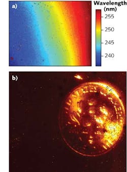
FPA showed some variation in responsivity of the peak wavelength, which varied between 237 and 256 nm (see figure). The sensor was easily able to image scenes illuminated with a 254 nm germicidal UV light. “The solar-blind regions of the ultraviolet spectrum offer a unique low-background window,” says Northwestern University professor Manijeh Razeghi. “This makes true solar-blind cameras at wavelengths like ours ideal for the sensitive detection of manmade UV emissions. In particular, they can be used for inspection of power lines to detect high-voltage breakdown, or to identify incoming missiles and provide an early warning.”
REFERENCE
1. E. Cicek et al., SPIE Optics + Photonics 2011 conference, San Diego, CA, paper 8155B-115 (Aug. 25, 2011).

Gail Overton | Senior Editor (2004-2020)
Gail has more than 30 years of engineering, marketing, product management, and editorial experience in the photonics and optical communications industry. Before joining the staff at Laser Focus World in 2004, she held many product management and product marketing roles in the fiber-optics industry, most notably at Hughes (El Segundo, CA), GTE Labs (Waltham, MA), Corning (Corning, NY), Photon Kinetics (Beaverton, OR), and Newport Corporation (Irvine, CA). During her marketing career, Gail published articles in WDM Solutions and Sensors magazine and traveled internationally to conduct product and sales training. Gail received her BS degree in physics, with an emphasis in optics, from San Diego State University in San Diego, CA in May 1986.