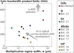
InAs electron APDs exceed conventional gain-bandwidth product limits

Electron avalanche photodiodes (e-APDs) are a new class of avalanche photodiode in which multiplication occurs entirely from the impact ionization of electrons. Theoretically, the maximum impulse response duration for an e-APD—equal to the sum of the electron and hole transit times across the multiplication region—remains constant regardless of its operational gain, meaning that e-APDs (unlike conventional APDs) should not be restricted by a gain-bandwidth product limit. These e-APDs have recently been demonstrated for II-VI and III-V material systems using mercury cadmium telluride (HgCdTe) and indium arsenide (InAs); however, the bandwidth of HgCdTe devices is limited to hundreds of megahertz and their low bandgap energy necessitates operation at 77 K.
By exploiting the fundamental properties of e-APDs and recent advances in InAs diode fabrication, researchers at Lancaster University (Lancaster, England) and the University of Sheffield (Sheffield, England) have made the first high-bandwidth, waveguide-coupled InAs e-APDs. The multiplication region width w has been optimized for both high bandwidth and high gain, leading to the demonstration of room-temperature-operation n-i-p type e-APDs with a 430 GHz gain-bandwidth product, as well as 580 GHz e-APDs operating at 77 K. This paves the way for future e-APDs that can achieve the terahertz gain-bandwidth products needed for next-generation communications and other high-speed detection applications. Contact Andrew Marshall at [email protected].
About the Author

Gail Overton
Senior Editor (2004-2020)
Gail has more than 30 years of engineering, marketing, product management, and editorial experience in the photonics and optical communications industry. Before joining the staff at Laser Focus World in 2004, she held many product management and product marketing roles in the fiber-optics industry, most notably at Hughes (El Segundo, CA), GTE Labs (Waltham, MA), Corning (Corning, NY), Photon Kinetics (Beaverton, OR), and Newport Corporation (Irvine, CA). During her marketing career, Gail published articles in WDM Solutions and Sensors magazine and traveled internationally to conduct product and sales training. Gail received her BS degree in physics, with an emphasis in optics, from San Diego State University in San Diego, CA in May 1986.