As it did in the 1980s when it developed an excimer laser designed from the ground up for optical lithography, Cymer (San Diego, CA) is aiming to capture virtually the entire market for next-generation lithographic light sources. In this case, though, “next generation” means extreme UV (EUV), and more precisely, the 13.5 nm wavelength. Of all EUV wavelengths, 13.5 nm has been chosen by the chipmaking industry as a future production light source because a practical process exists for creating 13.5 nm light at relatively high average powers.
This process involves focusing 10.6 µm light from a CO2 laser onto 30-µm-diameter falling droplets of tin, turning them to plasma and generating a pulse of EUV—and doing this at a 50 kHz rate for months at a time without degrading the surrounding EUV optics. Cymer’s high-volume manufacturing (HVM) laser-produced plasma (LPP) system is now close to achieving this reliability.
The CO2 laser in Cymer’s system produces up to 30 kW of pulsed output. The laser and its beam-transport system (BTS) are enclosed and interlocked to meet Class 1 laser requirements. The CO2 beam is delivered by the BTS to a vacuum vessel where the plasma is created. A multilayer-coated ellipsoidal mirror partially surrounding the small plasma cloud collects the emitted EUV light and passes it along to separate illumination optics housed within the wafer scanner (in which wafers are exposed and patterned). A HVM I (first-generation) wafer scanner operating at full source power would take several seconds to expose a 26 × 33 mm site on a wafer using 15 to 20 mJ/cm2 photoresist.
Excellent dose repeatability
A HVM I source running at a 50% duty cycle and a 40 kHz repetition rate was recently tested in Cymer’s San Diego labs under conditions simulating use with a wafer scanner. The usable average EUV power from the source was about 11 W, assuming a 5 sr solid angle, 50% collector reflectivity, 90% gas transmission, and 65% spectral-purity-filter transmission (such a filter is needed to eliminate any CO2 laser radiation from the final light output). With the source driven in a scanner-simulation mode, a dose repeatability distribution of between 0.03% and 0.05% within the exposure field was demonstrated for six wafers, showing that meeting the final production dose-stability requirement of better than ±0.20% 3σ is feasible.
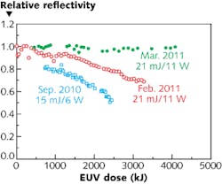
The plasma-creation area is an extreme environment, showering the ellipsoidal mirror with intense EUV radiation and tin-plasma debris with every laser shot; as a result, degradation of the ellipsoidal mirror and the overall EUV output have been prime concerns. However, through gas-flow techniques and improvements in the multilayer optical coatings, Cymer has been able to greatly reduce reflectivity loss over time (see figure).
Wall-plug power for the HVM I, with a 30 kW laser and a 105 W EUV output, is estimated to be around 500 kW, while for the next-generation HVM II, with a 40 kW laser and 250 W EUV output, the power consumption will be on the order of 450 kW due to improved radio-frequency (RF) efficiency for the laser. The later-generation HVM III will have a 50 kW laser, a 350 W EUV output, and a 500 kW wall-plug power.
Big machines, big collaboration
To move beyond the laboratory with its EUV light source, Cymer entered into a collaboration with ASML (Veldhoven, the Netherlands), a company that produces most of the lithographic wafer scanners bought each year by the world’s chipmakers. By itself, Cymer’s HVM source is quite large; however, it is dwarfed by ASML’s EUV scanner, which is intermediate in size between a living room and a small cottage. The partnership has produced crucial data for both companies, and for some of their customers as well (five HVM I sources are at customer facilities, all at unnamed leading chipmaker’s R&D facilities).

John Wallace | Senior Technical Editor (1998-2022)
John Wallace was with Laser Focus World for nearly 25 years, retiring in late June 2022. He obtained a bachelor's degree in mechanical engineering and physics at Rutgers University and a master's in optical engineering at the University of Rochester. Before becoming an editor, John worked as an engineer at RCA, Exxon, Eastman Kodak, and GCA Corporation.