HgTe-HgCdTe superlattice photodetector has high response in LWIR
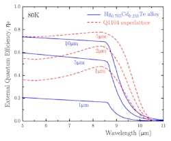
A superlattice of mercury telluride-mercury cadmium telluride (HgTe-HgCdTe) contains alternating layers of the two materials only nanometers thick; when used for IR photoconductive optical detectors, such a superlattice can have high absorption and good control of the cut-off wavelength. But until now there has been little data on the fabrication and use of such detectors in the longwave IR (LWIR). Researchers at the University of Western Australia (Crawley, Australia) and the Physikalisches Institut der Universität Würzburg (Würzburg, Germany) have fabricated two different examples of such detectors by molecular-beam epitaxy, comparing them to a non-superlattice detector of HgCdTe used as a control.
The differences in the two superlattice detectors were in the number of layers (120 versus 100) and the details of the elemental proportions in the layers under test. one of the superlattice detectors (Q1104) showed higher spectral quantum efficiencies as a function of thickness compared to the simple HgCdTe detector, partially because its absorption coefficient was more than four times higher. The spectral photoresponse of the other superlattice detector extended out well past 12 μm, compared to the less than 11 μm cutoff of the control. Contact John Dell at [email protected].

Gail Overton | Senior Editor (2004-2020)
Gail has more than 30 years of engineering, marketing, product management, and editorial experience in the photonics and optical communications industry. Before joining the staff at Laser Focus World in 2004, she held many product management and product marketing roles in the fiber-optics industry, most notably at Hughes (El Segundo, CA), GTE Labs (Waltham, MA), Corning (Corning, NY), Photon Kinetics (Beaverton, OR), and Newport Corporation (Irvine, CA). During her marketing career, Gail published articles in WDM Solutions and Sensors magazine and traveled internationally to conduct product and sales training. Gail received her BS degree in physics, with an emphasis in optics, from San Diego State University in San Diego, CA in May 1986.
