IR DETECTORS: Amorphous-silicon bolometers could surpass IR focal-plane technologies
CHARLES HANSON
During the last 35 years, thermal imaging has emerged as a critical enabling technology for modern warfare. However, initial interest in commercial and consumer applications was stymied by the cost, size, and weight of the imagers. Then, in the mid-1990s, Texas Instruments (TI; Dallas, TX) opened up the commercial market by introducing a barium-strontium titanate (BST) sensor—a ferroelectric device named for the composition of its sensitive material. Early commercial products included night-vision systems for automobiles, car-top thermal imagers for police, handheld thermal imagers for firefighters, and thermal security cameras.
Unfortunately, BST technology had performance limitations and was difficult to scale. The technology produced an image with quality superior to successor technologies, but it could not keep up with competitive improvements in sensitivity. Furthermore, because the BST detector was a hybrid device (fabrication required bonding a detector array to a separate readout integrated circuit) the ability to reduce pixel size was limited; and although the electronics could be miniaturized, system size was fixed by the need for an optomechanical chopper.
Microbolometers step in
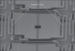
As a consequence of these limitations, vanadium-oxide (VOX) microbolometers began to displace BST detectors. A microbolometer focal-plane array (FPA) is an array of small VOX resistor elements or pixels, each thermally isolated from the environment and from each other by micromachined structures (see Fig. 1). When one of these elements (a pixel) absorbs infrared (IR) radiation, its temperature changes accordingly. Long, skinny legs provide thermal isolation so that the temperature change for a given flux change is maximized. The change in temperature alters the resistance of the pixel and a readout integrated circuit (ROIC) reads the resistance changes.
Microbolometers were initially developed by Honeywell (Morristown, NJ) and subsequently licensed to numerous others. As a result of the limitations of BST, TI began an independent microbolometer development based on amorphous silicon (a-Si) instead of VOX. Texas Instruments also developed a thin-film ferroelectric (TFFE) technology as a simple upgrade to overcome the limitations of BST. But even though BST production continued to lead the way after Raytheon acquired TI's defense business, microbolometers captured an increasing share of the rapidly growing market. In 2004 Raytheon sold the TI uncooled IR group with its BST, TFFE, and microbolometer technologies to L-3, who eventually discontinued BST production in 2009; TFFE technology development was discontinued about the same time because of manufacturing difficulties.
Amorphous silicon exceeds expectations
What is now the L-3 a-Si microbolometer began as a niche technology not intended for imaging. Initial estimates of its performance potential were modest. As development progressed, however, it was discovered that the temperature coefficient of resistance (TCR) could be increased far beyond that achievable with VOX, and 1/f noise could be suppressed using an appropriate deposition process. Furthermore, thermal isolation could be improved beyond that of competitive VOX devices since all the materials in the a-Si bolometer pixel were easily etched using standard CMOS processing.
The remaining barrier to competitive performance for L-3's a-Si bolometers was the mode of operation. Because the VOX microbolometer was developed when CMOS was in its infancy, integrating signals in the pixel unit cell was not an option due to insufficient capacitance. Furthermore, it was simpler to bias the pixels with a constant-current source and sample the signal voltages using a pair of orthogonal multiplexers—one to address a row and the other to select the column to be read. To minimize power dissipation, power was applied only during the time a given row was selected—a pulsed bias. This was a clever way to avoid high-power dissipation while eliminating the need for an amplifier in every unit cell. The amplifiers were instead located in the column circuitry—one for each column—which allowed plenty of room to make the amplifiers as large as necessary to achieve the requirements for low noise and linearity. The low impedance of VOX pixels matched this mode of operation well.
Texas Instruments began its a-Si microbolometer development much later, and it possessed leading-edge CMOS technology. Also, the impedance of a-Si was too large for easy implementation of the pulsed bias. As a result, L-3's a-Si microbolometers are now continuously biased at constant voltage, and signal current is integrated in the unit cell. Even with high-density CMOS circuitry the capacitance density was inadequate for efficient integration. The simple solution to this limitation was a switched-capacitor filter (S-C filter) that emulates a single-pole resistor-capacitor filter (R-C filter).
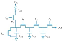
Operation is as follows for the unit cell of the ROIC: Current is integrated on capacitor Cint for a short time, while switch S1 is open; S1 is closed briefly to exchange charge and equalize voltage with Cxfr, then switch S2 is closed briefly so that Cxfr can exchange charge and equalize voltage with Cavg; finally, the integration capacitor Cint is reset and the process repeats, typically thousands of times between pixel reads (see Fig. 2).The signal-to-noise ratio is much the same as if the signal were integrated for the entire time between reads, but the filter suppresses both signal and noise. The benefit is that small capacitors can effectively integrate signal for a long time without exceeding the voltage limitations of the integrated circuit. Properly operated, the integration on Cint provides an ideal anti-aliasing pre-filter for the S-C filter, and the only noise is the kTC of the output capacitor Cavg. The pixel signal sits on Cavg, continuously updated at a rate of multiple kilohertz, and available for readout at the same rate.
While the use of the S-C filter permitted high-efficiency integration in the unit cell, it was initially insufficient to achieve performance parity with a multitude of VOX competitors. All bolometers have the property that the background current through the bolometer resistor is extremely large compared to typical signal currents. This limits the magnitude of the bias voltage, which limits bolometer performance. The column-based readout circuitry of pulse-biased bolometers could readily remove that current because of the large area available for signal processing. For a continuously biased array, however, the same task had to be done in the unit cell. An innovative but simple circuit that facilitated current subtraction simultaneously in all the unit cells changed that situation dramatically, and L-3's a-Si microbolometers became performance-competitive with the best of VOX devices.
The excellent uniformity of a-Si arrays means that a global current subtraction is adequate; that is, uniformity correction in the unit cell is unnecessary. The virtually continuous availability of the signal on Cavg is an important point, and this is unique to L-3. First, the high-speed update of the signal at that node means it is possible to read at an extremely high frame rate. Although standard ROICs are not designed with the bandwidth adequate to increase the frame rate much beyond the standard rate, sub-images can be read out at kilohertz frame rates. This can be useful for sensing short-duration events, provided the location of the event is known. The necessary accuracy of the location depends on the duration of the event, and detection of very fast events will mean that only a small part of the field of view can be read out sufficiently fast.
The second interesting capability of continuously biased bolometer technology is that it lends itself to the possibility of snapshot imaging. In the standard mode of operation all pixels are integrating signal simultaneously, and the S-C filters for all the pixels operate synchronously. Therefore all signals are simultaneously available on the Cavgcapacitors in the ROIC pixel unit cells. In standard operation the signals are read out line by line, because there is insufficient time between the integrations to read the entire array. However, the use of dual Cint capacitors in each unit cell, and a switch that permits accumulation of signal on one while the other is being read, will permit readout of the entire array with data captured simultaneously. This feature is uniquely possible with our constant-bias microbolometer technology.
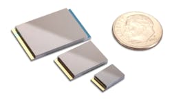
Our a-Si technology was born out of a desire for a small, lightweight, low-cost IR imager. It was recognized early that a significant contributor to size, weight, and cost would be packaging. Conventional packaging required handling individual detector arrays cut from silicon wafers. These individual arrays would each be mounted in a package, an IR-transmitting window would be attached to the top of the package, and the package would be evacuated while being heated and finally sealed. The L-3 approach simplifies this process through wafer-level packaging: The arrays on a silicon wafer are all sealed at one time; a second silicon wafer the same size as the array wafer is etched with rectangular cavities; the wafers are bonded together in vacuum; and the combined double-thickness wafer is diced into already packaged arrays (see Fig. 3).Microbolometer array technology has marched down the same road of pixel size reduction (and overall packaged size reduction) as other IR imaging technologies and this trend will surely continue. Other trends include improving the thermal isolation for better performance, and reduced thermal mass for faster response. Improving thermal isolation requires finer photolithographic resolution, which is pushing several manufacturers to look to semiconductor processing foundries to fabricate their devices due to the extremely high cost of fabrication equipment. Another approach to improving performance is via further increases in the active material TCR. Amorphous-silicon technology is particularly susceptible to that, because it is capable of a TCR in excess of 5%/°C while maintaining its other excellent properties. With this advantage, it is likely the a-Si microbolometer will soon establish itself as the premium technology for uncooled IR imaging.
Charles Hanson is CTO, infrared products, for L-3 Communications Electro-Optical Systems (L-3 EOS), 3414 Herrmann Dr., Garland, TX 75041; e-mail: [email protected]; www.l-3com.com.


