Last summer, applied physics professor A. Douglas Stone and colleagues at Yale University (New Haven, CT) published a study explaining the concept behind an anti-laser—a laser that works backwards, absorbing light at specific frequencies rather than emitting it.1 Less than a year later, the researchers have succeeded in fabricating a functioning anti-laser, which they call a coherent perfect absorber (CPA).
"Our results present a new approach for controlled absorption, either enhancing it to near-perfection at certain wavelengths, or suppressing it entirely," said Hui Cao, a Yale applied physics professor whose experimental group realized the CPA in close collaboration with Stone's theoretical group.2 "The technology portends several applications: more compact integrated silicon devices such as switches, modulators, and detectors; filtering or noise-suppression devices at particular wavelengths in biological- and chemical-sensing applications; and, possibly, tailored absorption of laser light in biological tissues or other media for targeted phototherapy or thermal experiments. Of course, these anti-laser applications will require much development before their impact can be properly evaluated."
A "loss" medium
Because time-reversal symmetry is a fundamental symmetry for classical electromagnetic theory and nonrelativistic quantum mechanics, it implies that a time-reversed analog for laser emission exists. Instead of applying a pump source to a gain medium in a laser cavity to create a population inversion and coherent laser emission, the Yale researchers replaced the gain medium with a "loss medium"—an absorptive material that can perfectly absorb the impinging coherent laser beams. This CPA requires that the frequency and field patterns of the incident light correspond exactly to the time-reversed emission patterns; if not, then absorption is reduced.
The simplest implementation of time-reversed lasing is a single-channel CPA, formed by an asymmetric cavity with a mirror at one end and a single input channel at the other. Several devices of this type have been realized such as asymmetric Fabry-Perot modulators, resonant cavity-enhanced photodetectors, and critically coupled resonators (that act as switches or filters); they typically have a ring geometry equivalent to two decoupled single-channel CPAs. However, at the time these devices were developed, people did not realize that they were demonstrating CPA.
The Yale researchers developed the concept of time-reversal of a laser and showed that CPA can be realized in any complex system with appropriate illumination conditions. As an example, they realized a two-channel CPA that requires two coherent input beams and achieves perfect absorption only when these two beams have the correct relative phase and amplitude. By adjusting the relative phase of the two input beams, they can also suppress the absorption by increasing the amount of light that escapes from the cavity. The device then functions as an absorptive interferometer, potentially useful as a modulator, detector, or phase-controlled optical switch.
Canceling the light
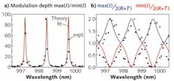
To fabricate the anti-laser, two collimated free-space counterpropagating beams (created by splitting a Ti:sapphire laser source) are directed to opposite surfaces of a 110-μm-thick silicon wafer that functions as a low-Q (with a Q of approximately 840) Fabry-Perot etalon. The separate output-beam intensities as well as the total output intensity are recorded by a spectrometer. In this configuration, the multiply scattered transmission from the left beam interferes destructively with the multiply scattered reflection from the right beam at the right interface, and vice versa at the left face. At the precise CPA condition, this leads to an ideal interference "trap" for the two beams, such that eventually the radiation is entirely dissipated by the interband absorption processes in the silicon. That is, as the relative input phase of the two beams is varied, the cavity cycles through a maximum output intensity to complete cancellation (or perfect absorption) of the two beams (see figure).
REFERENCES
1. Y.D. Chong et al., Physical Rev. Lett., 105, 053901 (July 2010).
2. W. Wan et al., Science, 331, 889–892 (February 2011).

Gail Overton | Senior Editor (2004-2020)
Gail has more than 30 years of engineering, marketing, product management, and editorial experience in the photonics and optical communications industry. Before joining the staff at Laser Focus World in 2004, she held many product management and product marketing roles in the fiber-optics industry, most notably at Hughes (El Segundo, CA), GTE Labs (Waltham, MA), Corning (Corning, NY), Photon Kinetics (Beaverton, OR), and Newport Corporation (Irvine, CA). During her marketing career, Gail published articles in WDM Solutions and Sensors magazine and traveled internationally to conduct product and sales training. Gail received her BS degree in physics, with an emphasis in optics, from San Diego State University in San Diego, CA in May 1986.
